Array substrate structure of display panel and method of making the same
- Summary
- Abstract
- Description
- Claims
- Application Information
AI Technical Summary
Benefits of technology
Problems solved by technology
Method used
Image

Examples
Embodiment Construction
[0019]To provide a better understanding of the present invention, preferred embodiments will be made in detail. The preferred embodiments of the present invention are illustrated in the accompanying drawings with numbered elements.
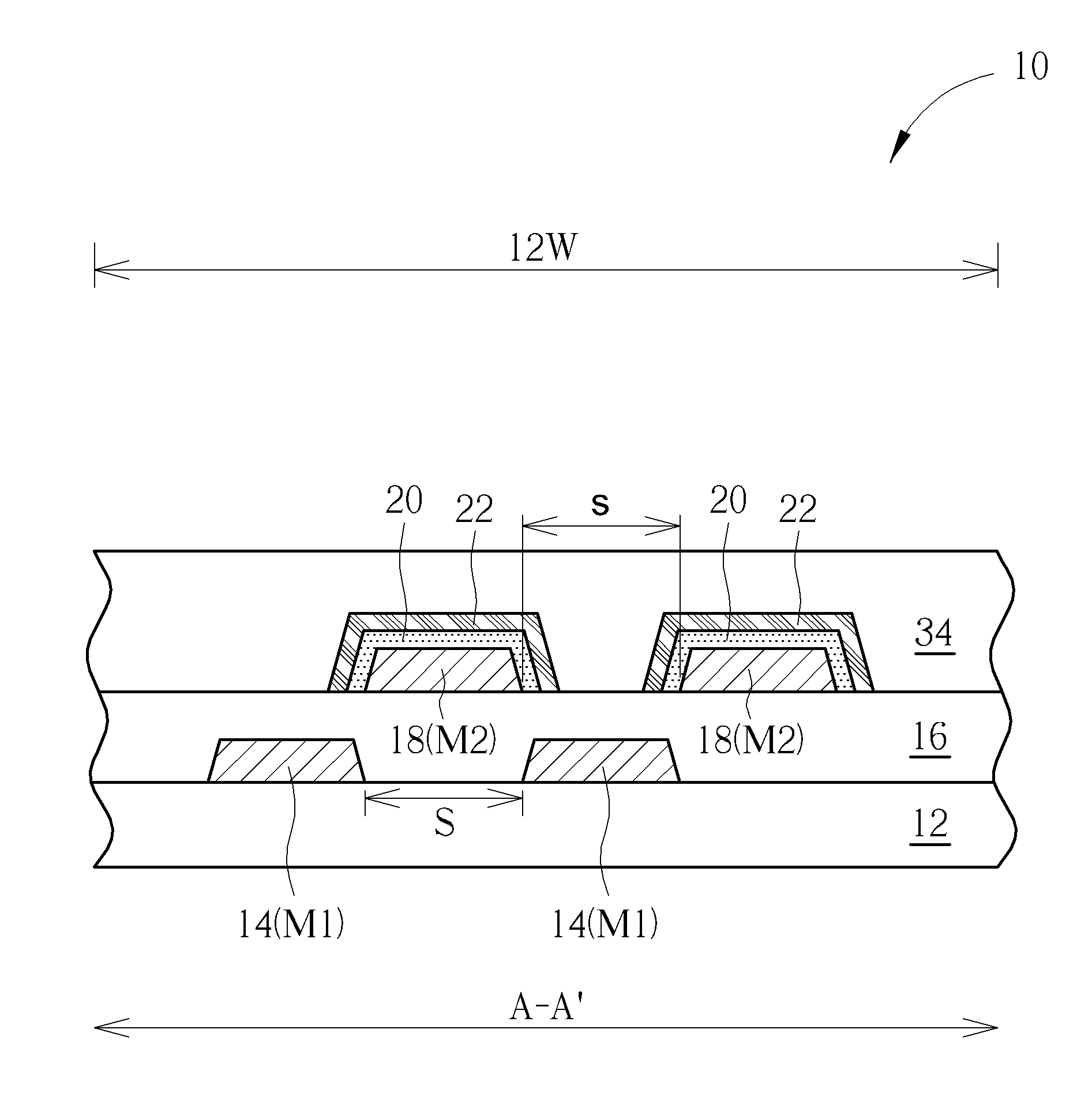
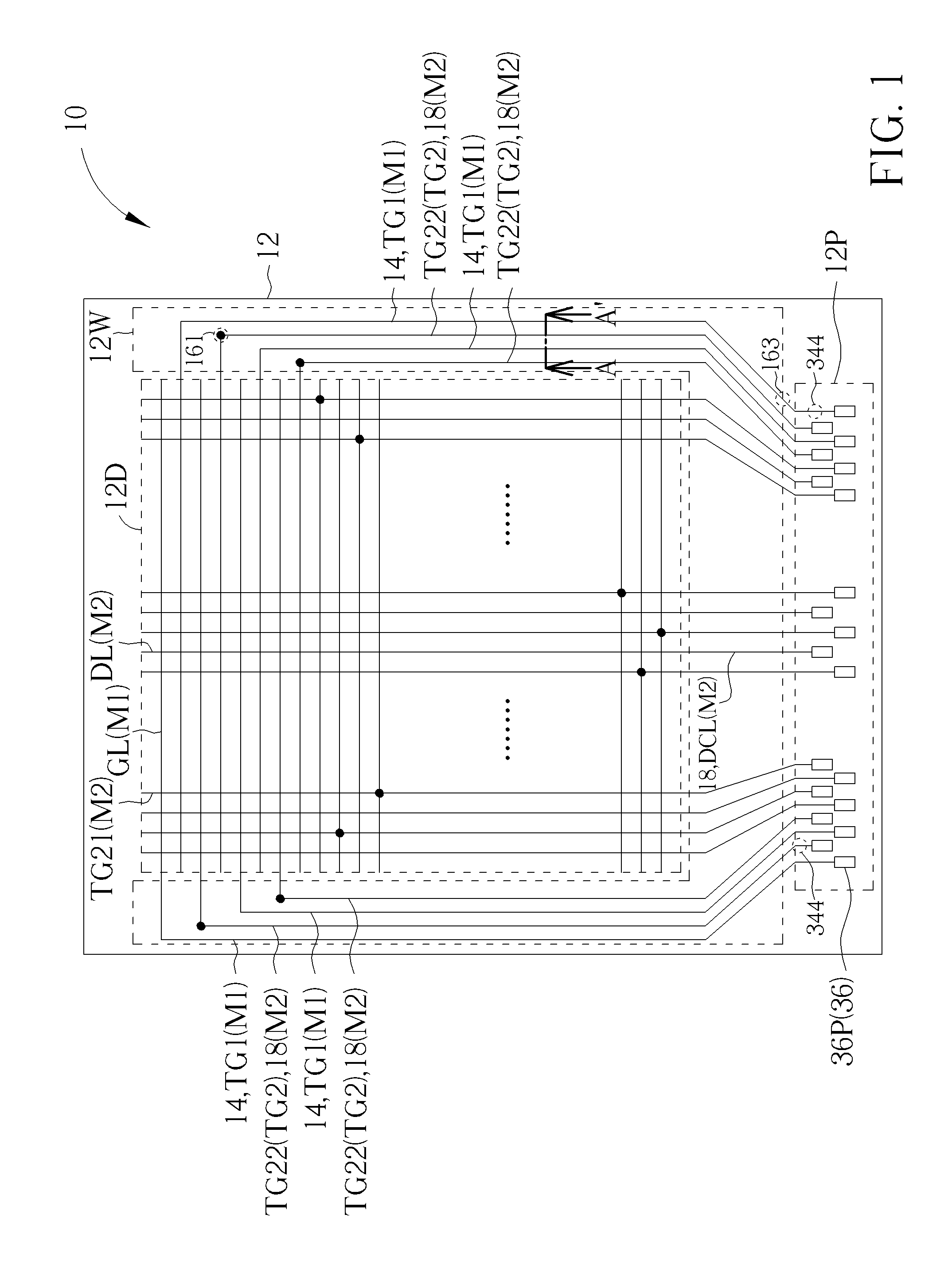
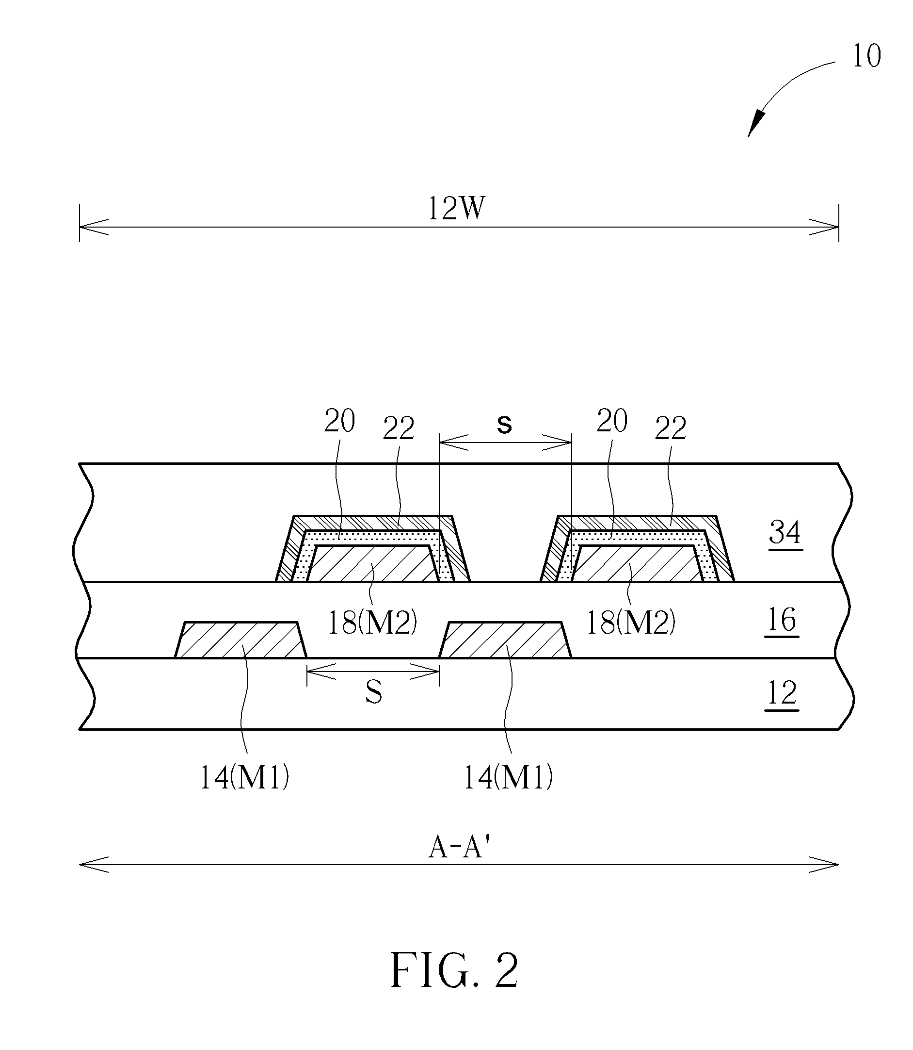
[0020]Please refer to FIGS. 1-2, FIGS. 1-2 are schematic diagrams illustrating an array substrate structure of a display panel according to a preferred embodiment of the present invention, wherein FIG. 1 is a top view of the array substrate structure of the display panel according to the preferred embodiment and FIG. 2 is a cross-sectional view taken along line A-A′ of FIG. 1. It should be noted that the preferred embodiment exemplarily provides an array substrate structure of a fringe field switching (FFS) liquid crystal display panel, but not limited to this. For example, the array substrate structure of the display panel can be an array substrate structure of any types of LCD panel, electroluminescent display panel and any types of display panel. As sho...
PUM
 Abstract
Description
Claims
Application Information
 - R&D
- Intellectual Property
- Life Sciences
- Materials
- Tech Scout
- Unparalleled Data Quality
- Higher Quality Content
- 60% Fewer Hallucinations
Browse by: Latest US Patents, China's latest patents, Technical Efficacy Thesaurus, Application Domain, Technology Topic, Popular Technical Reports.
© 2025 PatSnap. All rights reserved.Legal|Privacy policy|Modern Slavery Act Transparency Statement|Sitemap|About US| Contact US: help@patsnap.com