

Semiconductor device and method of manufacturing the same
a technology of semiconductor devices and semiconductors, applied in semiconductor devices, semiconductor/solid-state device details, electrical apparatus, etc., can solve the problems of reduced difficult formation of a deep hole, and increased difficulty in embedding metal in association, so as to improve the mechanical improve the yield and reliability of the wiring process, and increase the coupling strength of the connection pillar.
- Summary
- Abstract
- Description
- Claims
- Application Information
AI Technical Summary
Benefits of technology
Problems solved by technology
Method used
Image

Examples
Embodiment Construction
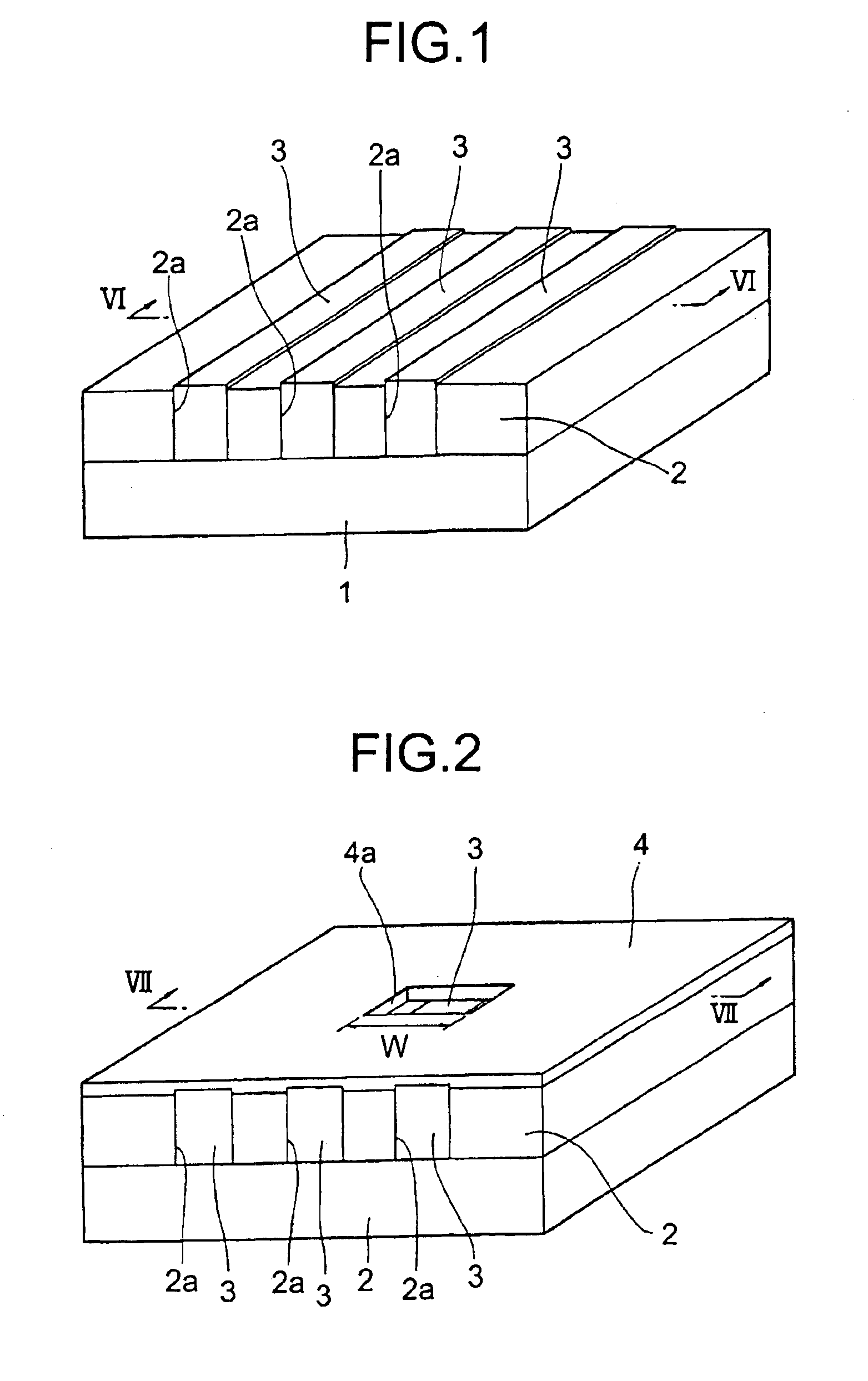
ment of the present invention;
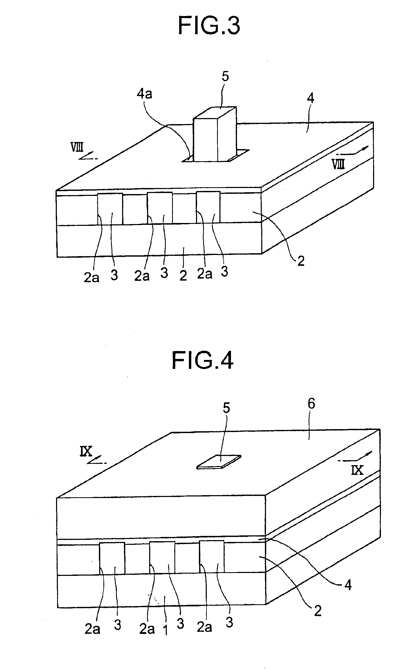
[0030]FIG. 4 is a perspective view describing the method of manufacturing the semiconductor device according to the embodiment of the present invention;
[0031]FIG. 5 is a perspective view describing the method of manufacturing the semiconductor device according to the embodiment of the present invention;
[0032]FIG. 6 is a sectional view taken on a line VI—VI of FIG. 1;
[0033]FIG. 7 is a sectional view taken on a line VII—VII of FIG. 2;
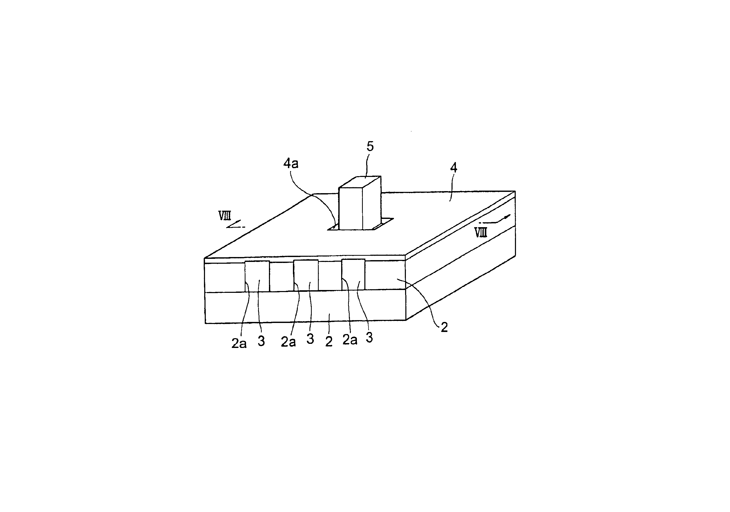
[0034]FIG. 8 is a sectional view taken on a line VIII—VIII of FIG. 3;
[0035]FIG. 9 is a sectional view taken on a line IX—IX of FIG. 4; and
[0036]FIG. 10 is a sectional view taken on a line X—X of FIG. 5.
DETAILED DESCRIPTION OF THE PREFERRED EMBODIMENTS
[0037]An embodiment of the present invention will be described below with reference to the attached drawings. By the way, the same symbols are given to the same or corresponding portions in all the drawings of the embodiment.
[0038]FIGS. 1 to 5 are the perspective views illustrati...
PUM
 Abstract
Description
Claims
Application Information