Antifuse having uniform dielectric thickness and method for fabricating the same

a technology of amorphous silicon and an antifuse, which is applied in the direction of semiconductor devices, electrical devices, semiconductor/solid-state device details, etc., can solve the problems of difficult to achieve high-level amorphous silicon, etc., and achieves the effect of facilitating the formation of silicides, improving the uniformity of antifuse materials, and ensuring the uniformity

Inactive Publication Date: 2006-07-06
DONGBU ELECTRONICS CO LTD
View PDF11 Cites 9 Cited by
  • Summary
  • Abstract
  • Description
  • Claims
  • Application Information

AI Technical Summary

Benefits of technology

[0013] Preferably, the filling layer comprises tungsten and has a recess that may be formed by depositing tungsten on a substrate or wafer (e.g., onto the lower metal layer), planarizing the tungsten (e.g., by chemical mechanical polishing, or CMP) to remove the tungsten from outside the contact and / or via hole, and etching part of the remaining tungsten using an etchant and / or cleaner comprising H2O2 to form the recess. The filling layer thus may partly fill the contact and / or via hole and compensate for the relatively high step coverage of the surface on which the amorphous silicon layer is formed. Therefore, the uniformity of the antifuse material (amorphous silicon) thickness can be improved and / or ensured. Further, since the recess in the filling layer may have a predetermined depth, the amorphous silicon layer may contact both lower and upper metal layers to facilitate the formation of a silicide (e.g., titanium silicide) with the lower and / or upper metal layer(s).

Problems solved by technology

Achieving a high uniformity of the antifuse material, amorphous silicon, is particularly difficult when it is deposited on an uneven surface such as in contact and / or via holes.

Method used


Image

  • Antifuse having uniform dielectric thickness and method for fabricating the same
  • Antifuse having uniform dielectric thickness and method for fabricating the same
  • Antifuse having uniform dielectric thickness and method for fabricating the same

Examples


Embodiment Construction

[0023] Hereinafter, preferred embodiments of the present invention will be described with reference to the accompanying drawings.

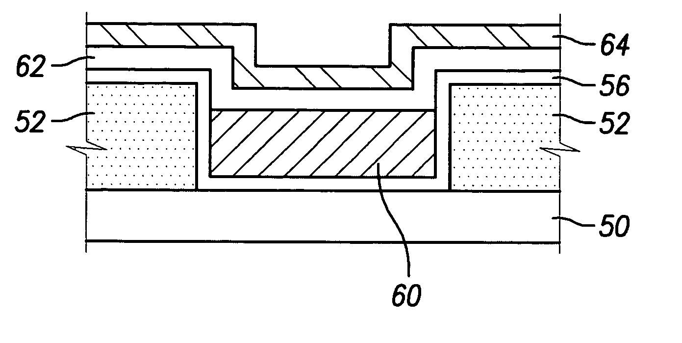
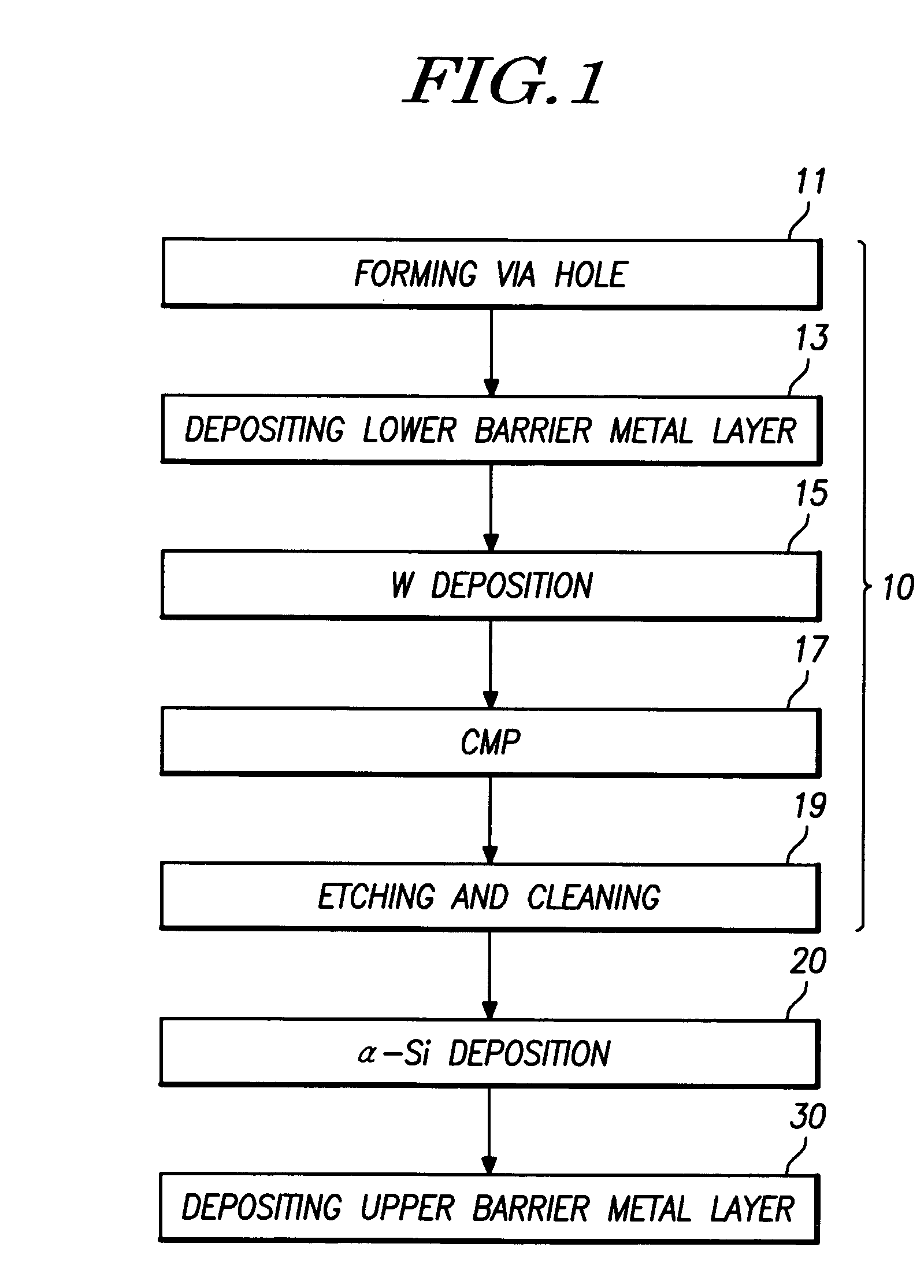
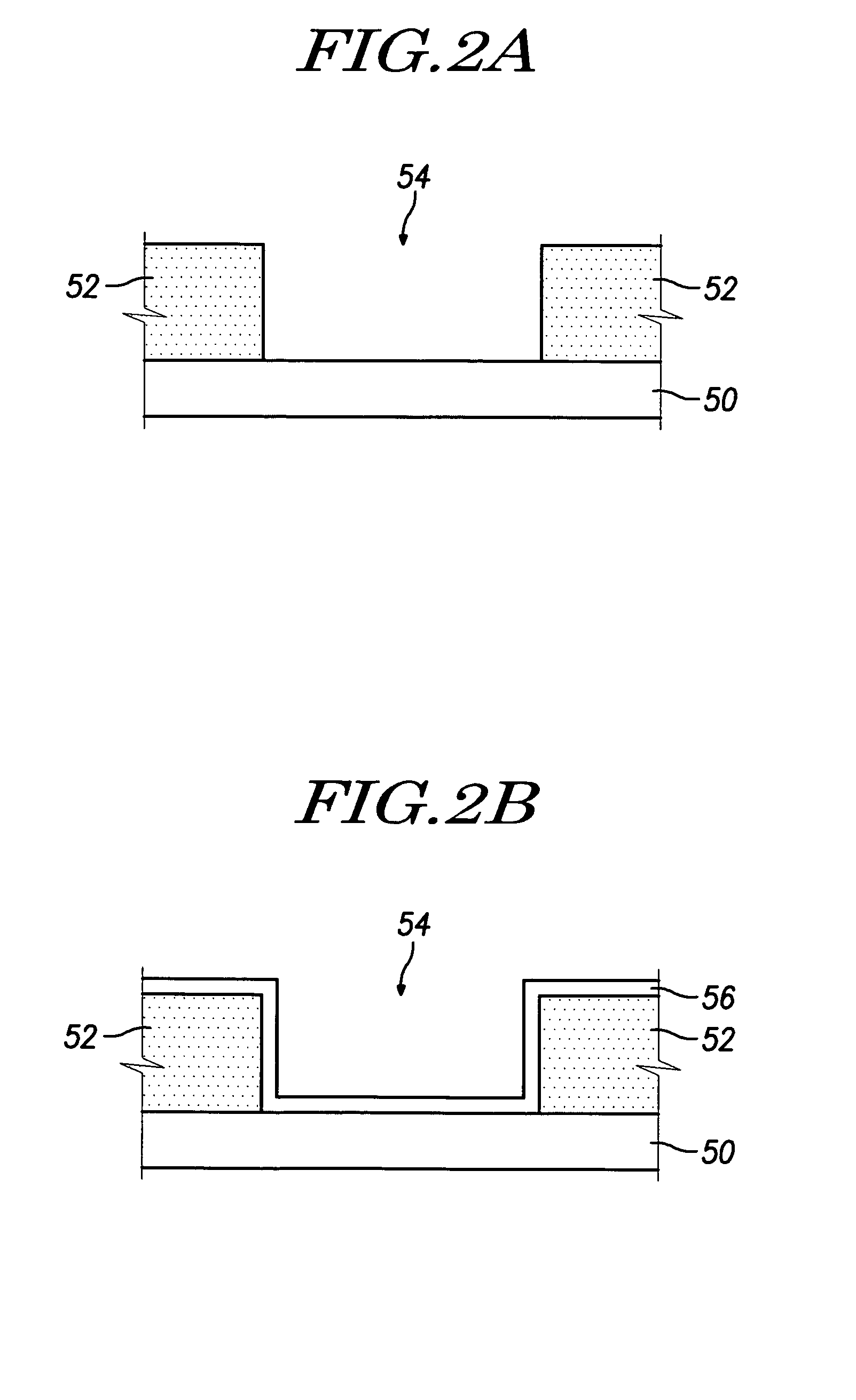
[0024] Referring to FIG. 1, a method for fabricating an antifuse according to the present invention may include contact forming step 10, antifuse material deposition step 20, and upper metal layer deposition step 30. In the contact forming step 10, a base for a programmable (or potential) connection structure (or antifuse) between overlying and underlying conductive layers that can be interconnected by the antifuse is formed. The overlying conductive layer may comprise a polysilicon layer (which may further have a metal silicide layer thereon) or a lower metal layer, and the underlying conductive layer may comprise an impurity diffusion layer (e.g., a source and / or drain terminal of a CMOS transistor, a base / emitter / collector terminal of a bipolar transistor, a buried bit line or word line in a memory, an electrode in a capacitor or an electrical connecti...


PUM

PropertyMeasurementUnit
resistanceaaaaaaaaaa
conductiveaaaaaaaaaa
depthaaaaaaaaaa

Abstract

Disclosed are an antifuse having a uniform amorphous silicon (antifuse material) thickness and a method for fabricating such an antifuse device. The antifuse is located between overlying and underlying conductive layers, and includes: a contact and/or via hole in an insulating layer on the underlying conductive layer; a lower metal layer contacting inner surfaces of the contact and/or via hole and a top surface of the insulating layer; a filling layer contacting the lower barrier metal layer and at least partially filling the contact and/or via hole; an antifuse material layer contacting a top surface of the filling layer and a part of the lower metal layer; and an upper metal layer on the antifuse material layer.

Description

CROSS-REFERENCE TO RELATED APPLICATION [0001] This application claims priority to and the benefit of Korean Patent Application No. 10-2004-117644, filed in the Korean Intellectual Property Office on Dec. 31, 2004, the entire contents of which are incorporated herein by reference. BACKGROUND OF THE INVENTION [0002] 1. Field of the Invention [0003] The present invention relates to an antifuse device having a uniform antifuse material thickness and a method for fabricating the same. [0004] 2. Description of the Related Art [0005] Field programmable gate arrays (FPGAs) that can be programmed by users to implement virtually any set of functions sometimes employ antifuse devices for programmable elements. Antifuse devices generally include a pair of conductive electrodes separated by a dielectric layer. Amorphous silicon or α-silicon is frequently used for the dielectric layer, and thus prior to programming, the antifuse tends to exhibit very high resistance (typically >109 Ω) between ...

Claims


Application Information

Patent Timeline
Patent Type & Authority Applications(United States)
IPC IPC(8): H01L29/00
CPCH01L23/5252H01L2924/3011H01L2924/0002H01L2924/00H01L21/82
Inventor PARK, KEUN SOO
Owner DONGBU ELECTRONICS CO LTD
Why Eureka
Try Eureka