Method of wafer level packaging and cutting

a technology of packaging and wafers, applied in the field of packaging and cutting, can solve the problems of reducing yield, reducing yield, and manual operation, and achieve the effects of reducing damage and contamination, reducing yield loss, and simplifying the cutting process

Inactive Publication Date: 2007-07-19
TOUCH MICRO SYST TECH
View PDF7 Cites 10 Cited by
  • Summary
  • Abstract
  • Description
  • Claims
  • Application Information

AI Technical Summary

Benefits of technology

[0008] The method of the invention may simplify the cutting process and diminish damage and contamination resulting from the cutting process. The method may apply to electronic device packages, micro-electromechanical systems (MEMS) device packages, and optical device packages. In addition, the method of the invention reduces the yield loss

Problems solved by technology

This packaging method needs individual operation, and even manual operation.
In addition, these products may be contami

Method used


Image

  • Method of wafer level packaging and cutting
  • Method of wafer level packaging and cutting
  • Method of wafer level packaging and cutting

Examples


Embodiment Construction

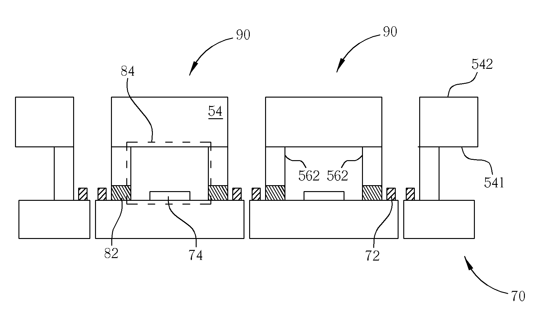
[0013] Hereinafter, an embodiment of the present invention will be described in detail with reference to the drawings. Please refer to FIG. 5 through FIG. 11. FIG. 5 through FIG. 11 are schematic diagrams illustrating a method of wafer level packaging and cutting according to a preferred embodiment of the invention. As shown in FIG. 5, a packaging wafer 50 is provided. The packaging wafer 50 comprises a transparent substrate 54 and a pattern 56, such as a silicon pattern, disposed on an upper surface 541 thereof. The pattern 56 defines a plurality of cavities 52 on the upper surface 541 of the packaging wafer 50. The above-mentioned transparent substrate 54 may comprise glass, quartz, or light transmissible plastic. In this preferred embodiment, the transparent substrate 54 is a glass substrate. As shown in FIG. 6, a pre-cutting process is performed upon a predetermined position of the packaging wafer 50. The pre-cutting process may be a wet wafer-cutting process, such as a wet etch...


PUM


Abstract

A packaging wafer having a plurality of cavities on an upper surface thereof is provided. A plurality of trenches is formed between the cavities, wherein the packaging wafer has a thickness greater than a depth of the trenches. The packaging wafer is bonded to an element wafer and a hermetical window is formed from each cavity. Then, a cutting process is performed and an unbound part of the packaging wafer is removed. Therefore, a wafer level package is formed. Finally, the wafer level package is divided into a plurality of individual packages.

Description

BACKGROUND OF THE INVENTION [0001] 1. Field of the Invention [0002] The invention relates to a method of packaging and cutting, and more particularly, to a method of wafer level packaging and cutting. [0003] 2. Description of the Prior Art [0004] A packaging process of semiconductor devices is an important step in back-end stages of semiconductor device manufacture. Packaging provides the semiconductor device with protection, heat dissipation, electricity, or connection to other components for compatibility with next level assembly. Please refer to FIG. 1 through FIG. 4. FIG. 1 through FIG. 4 illustrate a conventional method of die packaging. As shown in FIG. 1, a wafer 10 having a plurality of devices 12 on an upper surface thereof is provided. The wafer 10 is divided into a plurality of dies 16 for subsequent packaging. As shown in FIG. 2, a cap wafer 20 is provided. The cap wafer 20 is cut into a plurality of packaging caps 22 that have proper size and shape corresponding to the ...

Claims


Application Information

Patent Timeline
IPC IPC(8): H01L21/00
CPCB81C1/00873H01L2924/16235
Inventor WANG, SHUN-TA
Owner TOUCH MICRO SYST TECH
Why Eureka
Try Eureka