Semiconductor manufacturing equipment

a manufacturing equipment and semiconductor technology, applied in the direction of total factory control, programme control, instruments, etc., can solve the problems of not being able to specify, the manufacturing method has become more complicated, and noise (variation) such as white noise is included, so as to facilitate the detection and diagnosis of faults, simplify operation procedures, and accelerate the effect of taking countermeasures

Active Publication Date: 2013-07-04
HITACHI HIGH-TECH CORP
View PDF3 Cites 25 Cited by
  • Summary
  • Abstract
  • Description
  • Claims
  • Application Information

AI Technical Summary

Benefits of technology

[0031]The aspects of the present invention makes it easier to detect and diagnose a fault in semiconductor manufacturing equipment and processing (process) and also makes it faster to take countermeasures.
[0032]In particular, equipment data which is used for fault detection and diagnosis and which has been acquired at a short sampling interval may have any signal change and there is no need of dividing up a calculation method in accordance with whether or not there is correlation between signals, whether or not there is variation or noise, whether it is large or small, and whether signal intensity difference is large or small, which can therefore simplify operation procedures and also makes it easier to install thi

Problems solved by technology

In addition, a manufacturing method has become more complicated.
Moreover, in a signal obtained by actually monitoring the equipment, noise (variation) such as white noise is included.
Moreover, appearing waveform patterns are various, and it is also not necessarily possible to specify beforehand what waveform pattern occurs.
This does not make it p

Method used


Image

  • Semiconductor manufacturing equipment
  • Semiconductor manufacturing equipment
  • Semiconductor manufacturing equipment

Examples


first embodiment

[0113]An outline of a semiconductor manufacturing equipment monitoring method according to the invention in the semiconductor manufacturing equipment will be described, referring to FIG. 8.

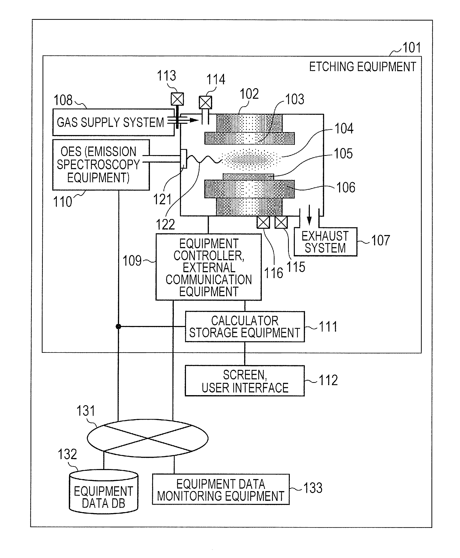
[0114]Configuration of the semiconductor manufacturing equipment 601 is the same as that shown in FIG. 6. The equipment monitoring processing is executed by the calculator-storage device 111 of the equipment in this embodiment.

[0115]In the semiconductor manufacturing equipment 601, wafer processing is carried out a plurality of times, and output signals of each equipment controller 611 and each in-processing sensor 621 are inputted into the calculator-storage device 111 via the equipment controller-outside communication equipment 109 and stored into the device data DB 132. The calculator-storage device 111 acquires from the device data DB 132 various signals as the stored equipment data for the number of times of processing, that is, data obtained by various signals×the number of times of processi...

second embodiment

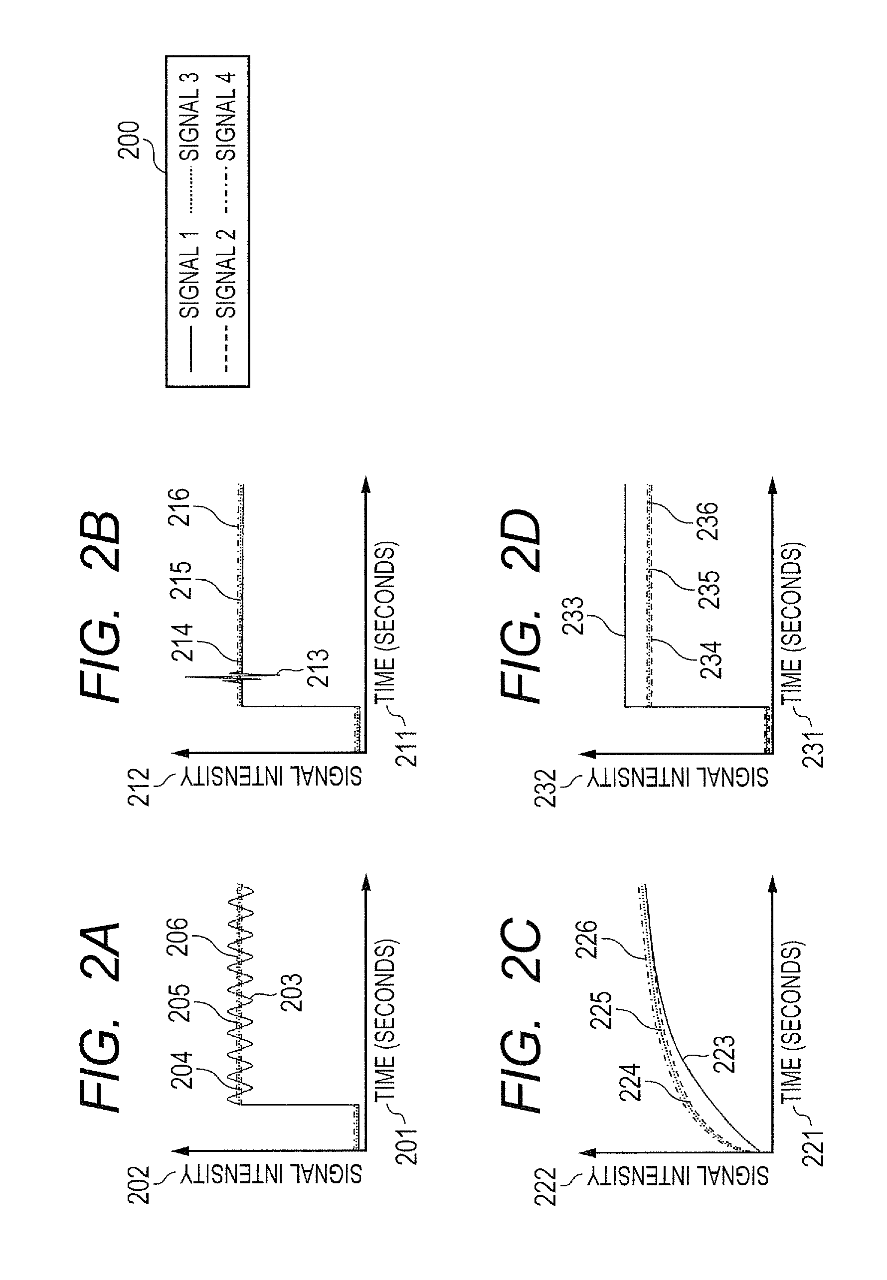
[0130]A method of arranging in the feature space each of the signals subjected to the 12 times of processing shown in FIG. 18 and extracting characteristic waveform patterns included in the signals are shown. The signal intensity of each signal shifts in a positive direction every process processing, and further hunting occurs near 15 seconds, 35 seconds, 55 seconds, and 75 seconds for the signals #001, 1811, #0041814, #0071817, and #0101820. There is delayed start from 0 seconds, i.e., a start point of analysis target for the signals #0011811, #0041814, #0071817, and #0101820. The delay increases in order of #0011811, #0041814, #0071817, and #0101820. Due to this delay, there is correlation between the signals for the four signals.

[0131]Indicated in this embodiment is that, regardless of whether or not there is correlation between the signals over the time points, by the inter-time-point principal component analysis IT-PCA, the inter-signal multi-dimensional scaling IS-MDS, and the...

third embodiment

[0143]Illustrated in this embodiment are examples of a method of performing fault detection and display of analysis results onto the screen-user interface.

[0144]Fault detection processing is identifying a faulty signal by determining arrangement relationship between a plurality of signals in a feature space which is defined as a principal component score in the inter-time-point principal component analysis IT-PCA and is defined as an MDS map in the inter-signal multi-dimensional scaling IS-MDS. The arrangement relationship between the plurality of signals in the feature space is, for example, the plots of the principal component scores shown in FIGS. 11A and 11B and FIG. 20 and the plots of the MDS maps shown in FIGS. 15A and 15B and FIGS. 23A to 23C.

[0145]Here, a method of fault determination for one principal component score will be described.

[0146]FIG. 26A shows distribution of signals with the second principal component pc2 calculated by the inter-time-point principal component ...


PUM


Abstract

Semiconductor manufacturing equipment includes: a controller controlling driving and processes of various parts of the semiconductor manufacturing equipment, and a sensor monitoring each physical amount in the semiconductor manufacturing equipment or a status of each chemical response amount; a database; and an arithmetic section executing: processing of reading out equipment data, calculating a correlation matrix between time points based on a plurality of pieces of signal data to be compared, calculating eigen values and eigen vectors from the correlation matrix, and calculating principal component scores by principal component analysis; processing of comparing magnitudes of the eigen values of the principal components, arranging the eigen values in descending order to display a list thereof; and processing of displaying a scatter diagram where the principal component scores of the respective signals are plotted in a feature space selecting the principal component corresponding to the eigen value having a contribution ratio.

Description

CLAIM OF PRIORITY[0001]The present application claims priority from Japanese application serial no. JP2011-288506, filed on Dec. 28, 2011, the content of which is hereby incorporated by reference into this application.BACKGROUND OF THE INVENTION[0002]1. Technical Field of the Invention[0003]The present invention relates to semiconductor manufacturing equipment, which includes equipment and a sensor monitoring statuses of various portions at time of equipment operation, including equipment which performs process processing by acquiring a map permitting quantitative judgment of waveform similarity based on compared values (matrix) between processing by use of equipment monitor signal data (waveforms) during a plurality of wafer processing, and which monitors the semiconductor manufacturing equipment.[0004]The invention more specifically relates to a function of quantifying difference between signals even under the presence of signals which cannot have correlation between the signals a...

Claims


Application Information

Patent Timeline
IPC IPC(8): G05B19/18
CPCG05B19/4184G05B2219/45031G05B2219/32191Y02P90/02
Inventor MORISAWA, TOSHIHIROSHIRAISHI, DAISUKEINOUE, SATOMIKAGOSHIMA, AKIRA
Owner HITACHI HIGH-TECH CORP
Why Eureka
Try Eureka