

Switch apparatus switching between basic input output system chip and diagnostic card
- Summary
- Abstract
- Description
- Claims
- Application Information
AI Technical Summary
Benefits of technology
Problems solved by technology
Method used
Image

Examples
Embodiment Construction
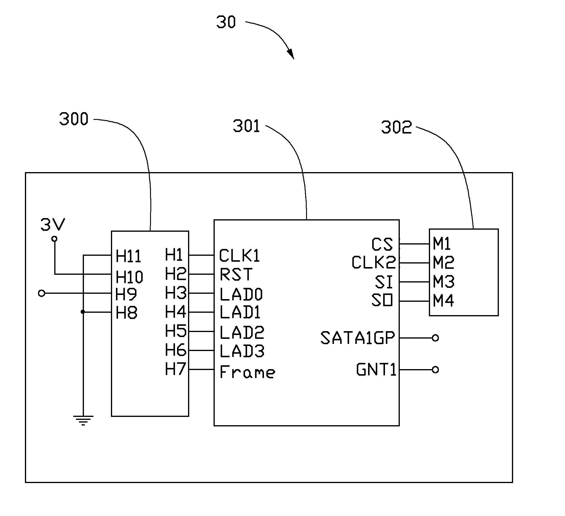
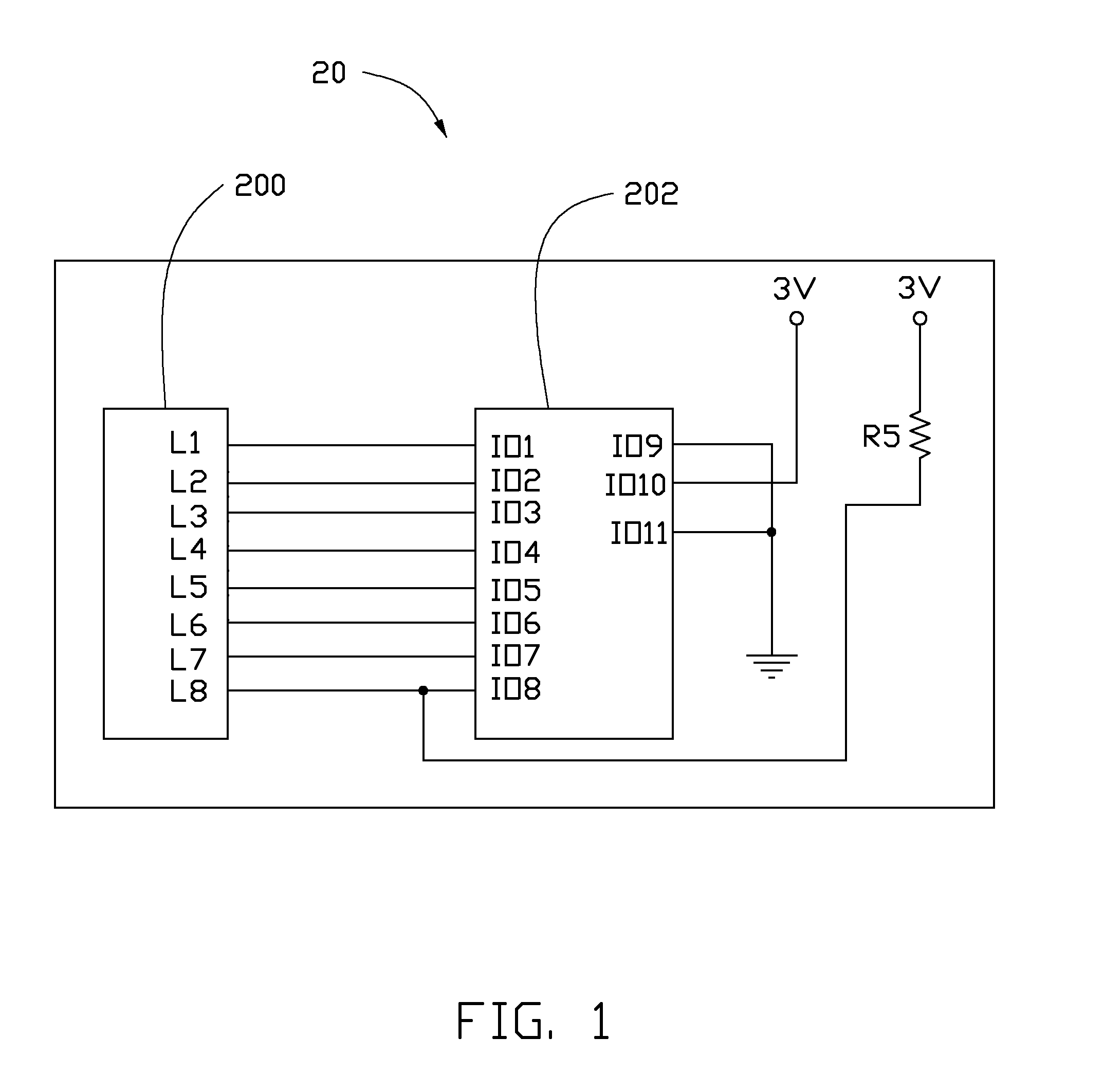
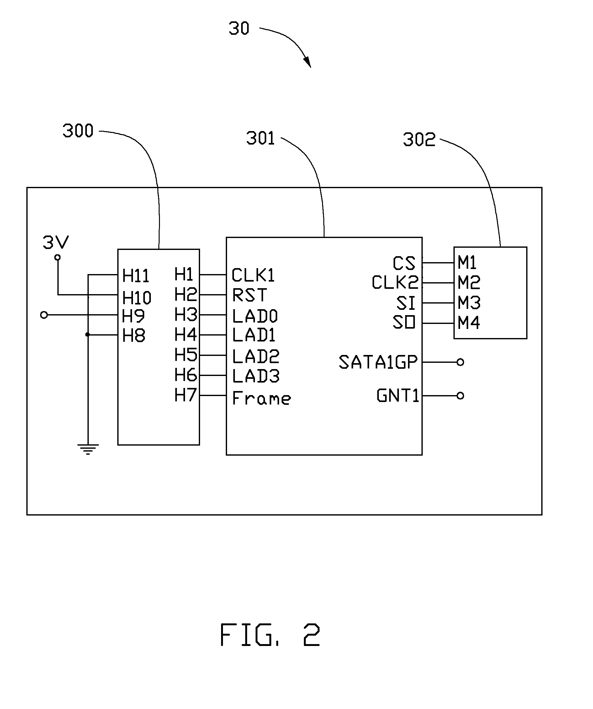
[0011]FIGS. 1 to 3 illustrate an embodiment of a switch apparatus which can switch between a first basic input output system (BIOS) chip 302 and a second BIOS chip 202 of the present disclosure. The switch apparatus includes a first connector 300, a platform controller hub (PCH) chip 301, and a switch circuit 303. The first connector 300, the PCH chip 301, the first BIOS chip 302, and the switch circuit 303 are all arranged on a motherboard 30. The second BIOS chip 202 is arranged on a diagnostic card 20.
[0012]The diagnostic card 20 further includes a second connector 200, and a resistor R5. When the motherboard 30 is in debugging mode, the second BIOS chip 202 is employed to bootstrap the motherboard 30. The second connector 200 is coupled to the second BIOS chip 202 through the low point count (LPC) bus. A pin IO1 of the second BIOS chip 202 is connected to a pin L1 of the second connector 200, to transmit a clock signal to the second connector 200. A pin IO2 of the second BIOS ch...
PUM
 Abstract
Description
Claims
Application Information