

Dual gate oxide trench mosfet with channel stop trench
a technology of oxide trenches and mosfets, which is applied in the direction of basic electric elements, electrical equipment, semiconductor devices, etc., can solve the problems of expensive and time-consuming five to six masking processes, and achieve the effects of reducing junction termination breakdown, improving uis capability, and saving space occupied by junction termination
- Summary
- Abstract
- Description
- Claims
- Application Information
AI Technical Summary
Benefits of technology
Problems solved by technology
Method used
Image

Examples
embodiments
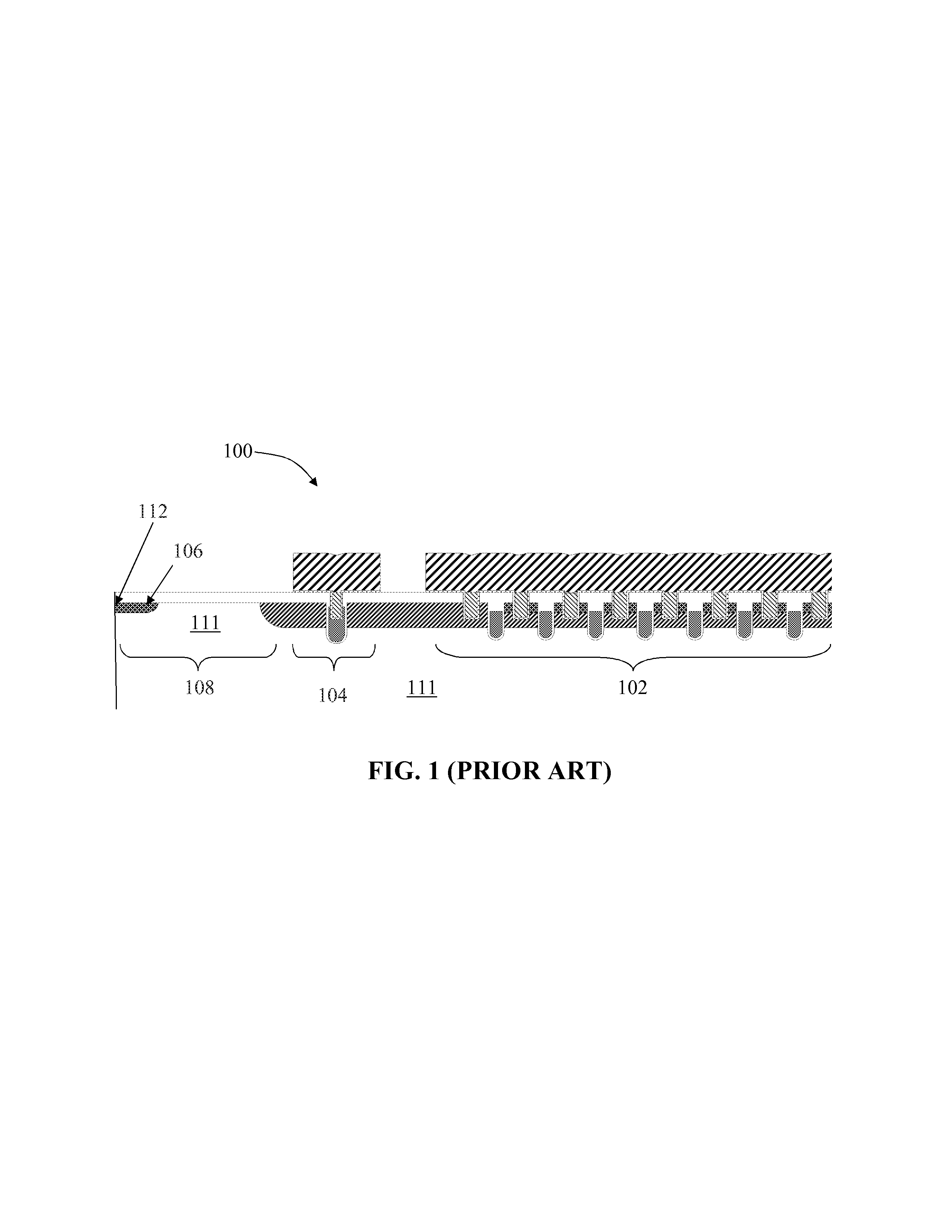
[0025]In embodiments of the present invention, the existing junction termination in a conventional trench MOSFET can be replaced with a thick gate oxide in the gate runner area to terminate the active cell area, which eliminates junction termination breakdown, improves the UIS capability, and saves space occupied by the junction termination because the oxide requires much less space than a conventional junction termination. In addition, reverse recovery is improved by confining the built-in body diode to the active area.
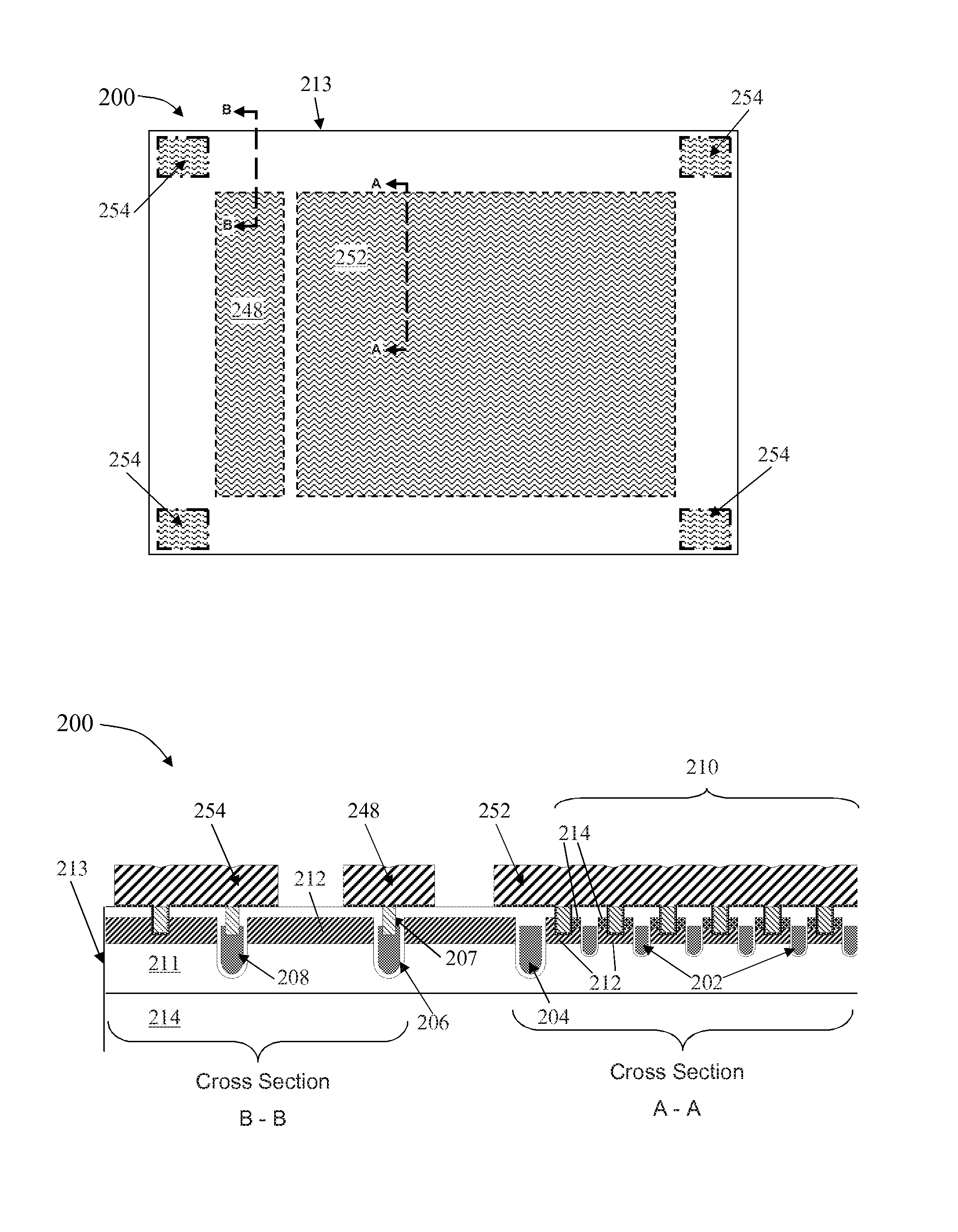
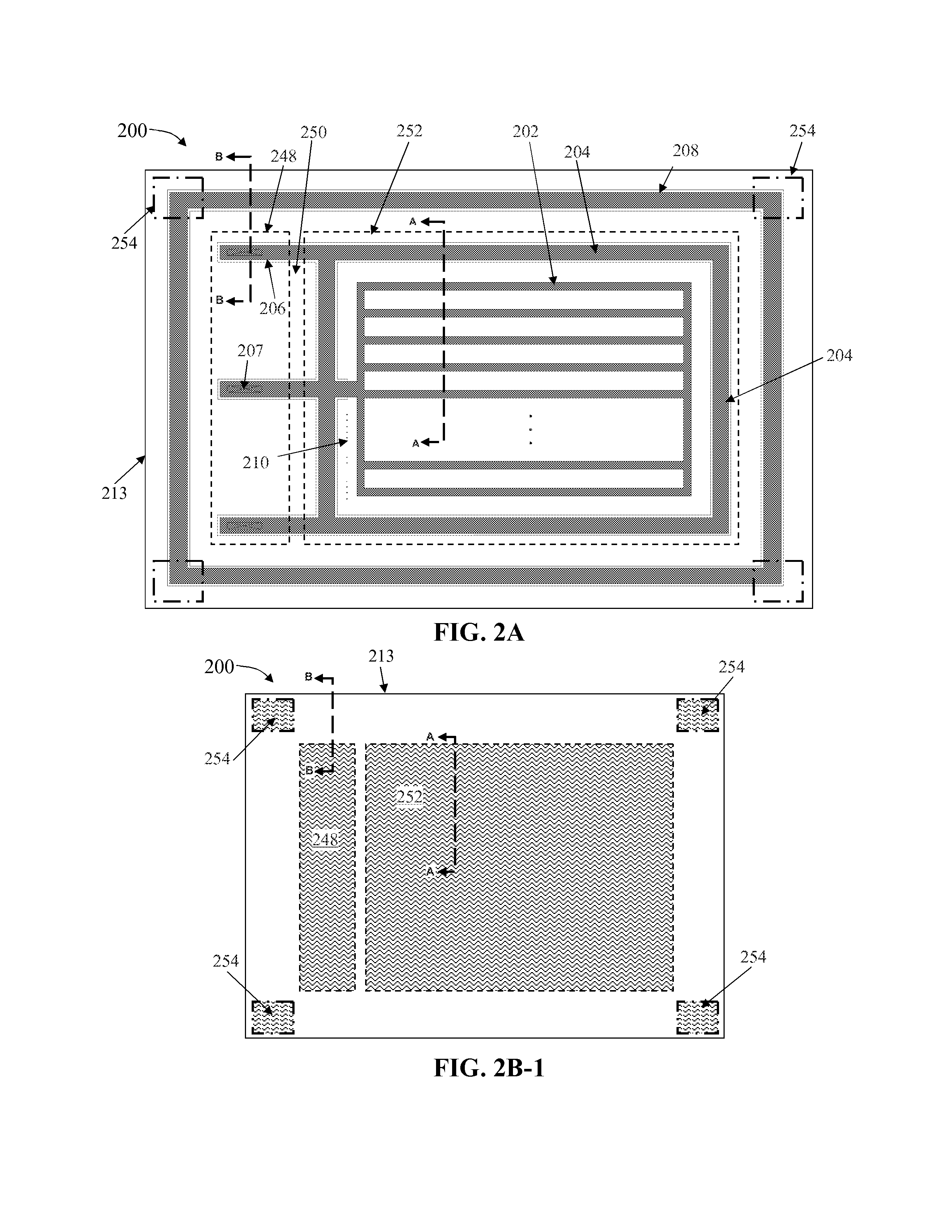
[0026]FIG. 2A is a top view of a layout of the dual gate oxide trench MOSFET 200 of a first embodiment of the present invention and FIG. 2B-2 is a cross-sectional view of the dual gate terminated trench MOSFET 200 along the lines A-A and B-B. The method for making the oxide termination trench MOSFET 200 only requires four masks: a trench mask, a gate oxide mask, a contact mask and a metal mask, which is described later in FIGS. 4A-4R.
[0027]As shown in FIGS. 2A and 2B...
PUM
 Abstract
Description
Claims
Application Information