
Oxide terminated trench mosfet with three or four masks

a trench mosfet and oxide technology, applied in the direction of semiconductor devices, electrical equipment, transistors, etc., can solve the problems of expensive and time-consuming five to six mask process, and achieve the effect of reducing junction termination breakdown, improving uis capability, and saving space occupied by junction termination

Active Publication Date: 2012-05-31
ALPHA & OMEGA SEMICON INC
View PDF1 Cites 28 Cited by
  • Summary
  • Abstract
  • Description
  • Claims
  • Application Information

AI Technical Summary

Benefits of technology

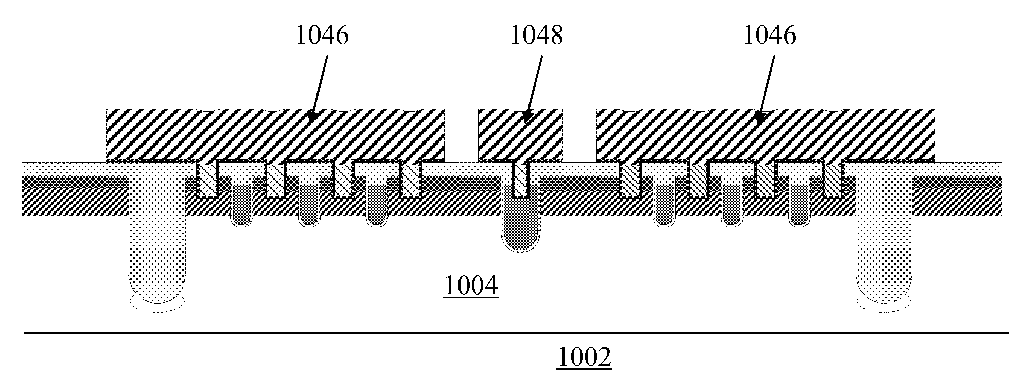
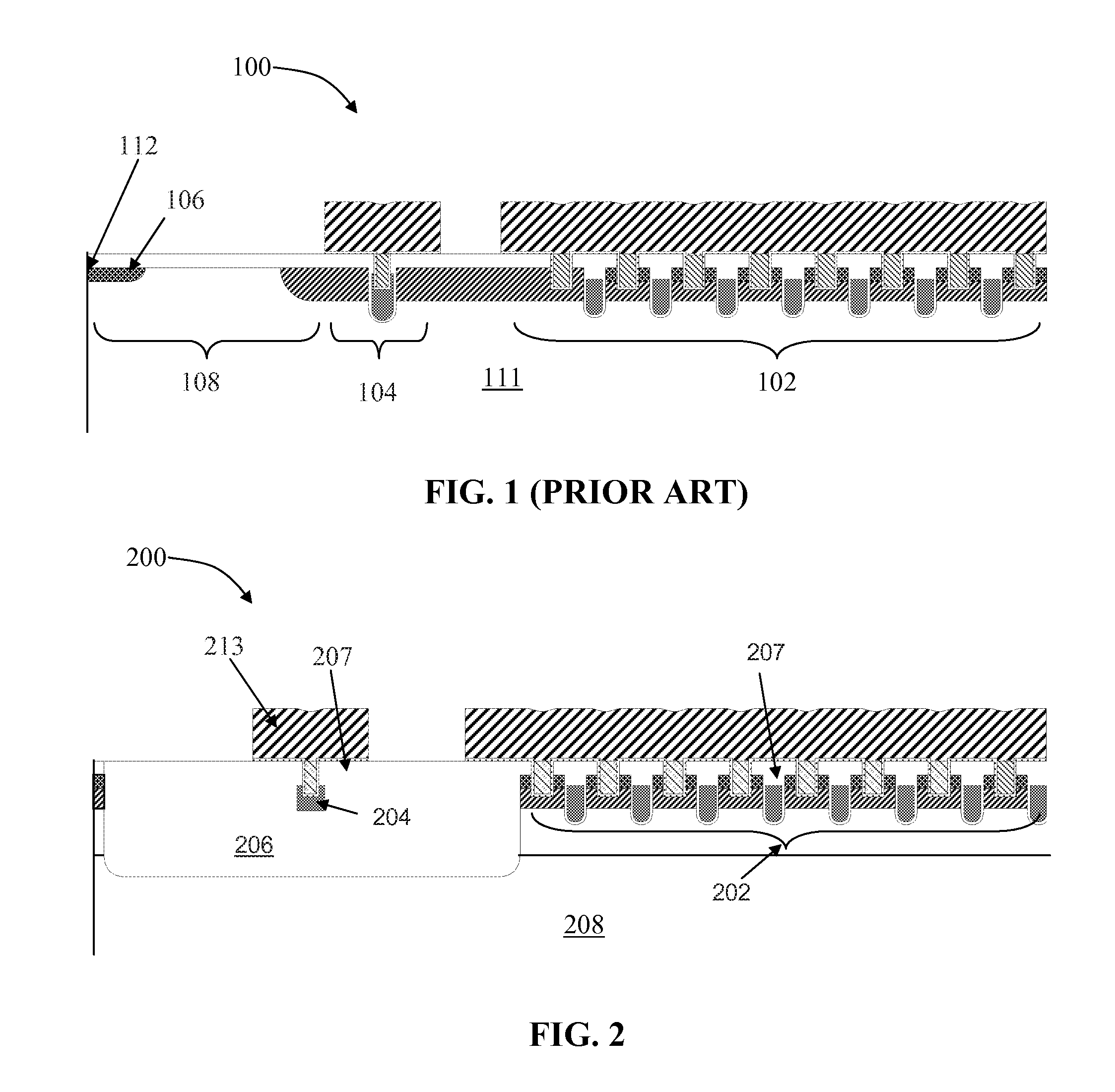
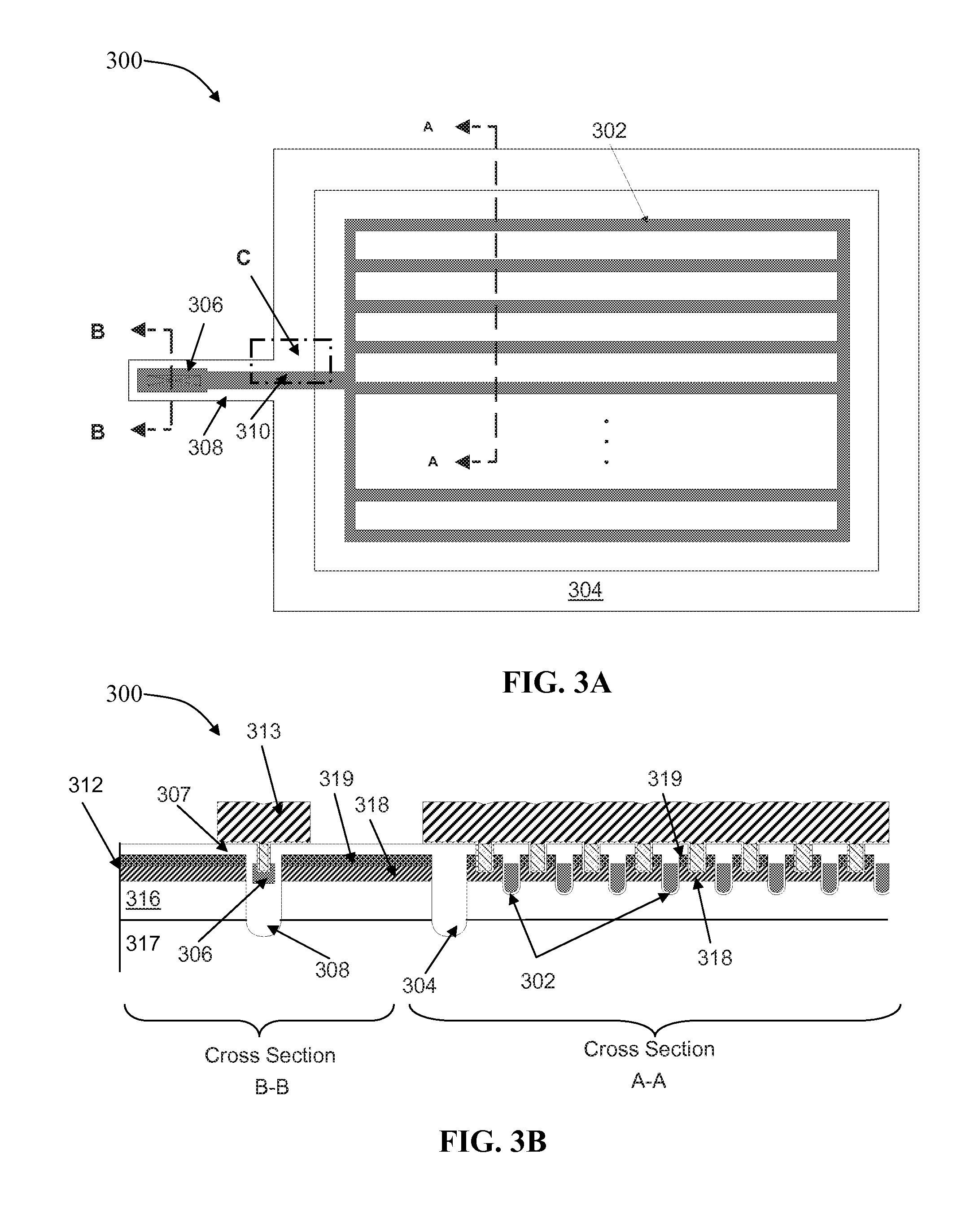
[0027]In embodiments of the present invention, the junction termination in a conventional trench MOSFET is replaced with an oxide termination which eliminates junction termination breakdown, improves the UIS capability, and saves space occupied by the junction termination because the oxide requires much less space than a conventional junction termination. In addition, reverse recovery is improved by confining the built-in diode to the active area.
[0059]As may be seen from the foregoing description, embodiments of the present invention allow for manufacture of trench MOSFET devices using fewer masks than conventional processes. The resulting structure eliminates junction termination breakdown, improves UIS capability, and saves space occupied by the junction termination because the oxide takes up much less space than a conventional junction termination. In addition, reverse recovery is improved by confining the built-in body diodes to the active area.

Problems solved by technology

However, a conventional method of making such a trench DMOS field effect transistor requires a five to six masks process that is expensive and time consuming

Method used


Image

  • Oxide terminated trench mosfet with three or four masks
  • Oxide terminated trench mosfet with three or four masks
  • Oxide terminated trench mosfet with three or four masks

Examples


embodiments

[0027]In embodiments of the present invention, the junction termination in a conventional trench MOSFET is replaced with an oxide termination which eliminates junction termination breakdown, improves the UIS capability, and saves space occupied by the junction termination because the oxide requires much less space than a conventional junction termination. In addition, reverse recovery is improved by confining the built-in diode to the active area.

[0028]According to a first embodiment, a gate runner is located in the oxide termination. FIG. 2 is a cross-sectional view of an oxide termination trench MOSFET 200. As shown in FIG. 2, the oxide termination trench MOSFET 200 includes active cells 202 located in an active region and a gate runner 204 positioned inside a large oxide filled trench 206 that is located in a termination region. A dielectric 207 such as Borophosphosilicate glass (BPSG), and / or the large oxide-filled trench 206 can be used to insulate gate pad 213 from the drain v...


PUM


Abstract

An oxide termination semiconductor device may comprise a plurality of gate trenches, a gate runner, and an insulator termination trench. The gate trenches are located in an active region. Each gate trench includes a conductive gate electrode. The insulator termination trench is located in a termination region that surrounds the active region. The insulator termination trench is filled with an insulator material to form an insulator termination for the semiconductor device. The device can be made using a three-mask or four-mask process.

Description

CLAIM OF PRIORITY[0001]This application is a continuation of and claims the priority benefit of commonly-assigned, co-pending U.S. patent application Ser. No. 12 / 731,112 entitled “OXIDE TERMINATED TRENCH MOSFET WITH THREE OR FOUR MASKS” to Sik Lui, filed Mar. 24, 2010, the entire disclosures of which are incorporated herein by reference.FIELD OF THE INVENTION[0002]This invention generally relates to trench metal oxide semiconductor field effect transistors (MOSFETS) and more particularly to oxide terminated trench MOSFETs and a method of forming such devices with three or four masks.BACKGROUND OF THE INVENTION[0003]A DMOS (Double diffused MOS) transistor is a type of MOSFET (Metal Oxide Semiconductor Field Effect Transistor) that uses two sequential diffusion steps aligned to the same edge to form the channel region of the transistor. DMOS transistors are often high current devices for low and high voltages, used either as discrete transistors or as components in power integrated ci...

Claims


Application Information

Patent Timeline
Patent Type & Authority Applications(United States)
IPC IPC(8): H01L29/78
CPCH01L29/0638H01L29/0649H01L29/0661H01L29/0878H01L29/407H01L29/41766H01L29/4236H01L29/4238H01L29/456H01L29/66734H01L29/7811H01L29/7813H01L29/66666H01L29/7827H01L21/76224H01L29/0653H01L21/3081H01L21/31H01L21/32133H01L27/088
Inventor LUI, SIKBHALLA, ANUP
Owner ALPHA & OMEGA SEMICON INC
Learn More