
Method for making dual gate oxide trench MOSFET with channel stop using three or four masks process

a technology of trench mosfet and channel stop, which is applied in the direction of semiconductor devices, basic electric elements, electrical equipment, etc., can solve the problems of expensive and time-consuming five to six mask process, and achieve the effect of reducing junction termination breakdown, improving uis capability, and saving space occupied by junction termination

Active Publication Date: 2013-03-12
ALPHA & OMEGA SEMICON INC
View PDF8 Cites 21 Cited by
  • Summary
  • Abstract
  • Description
  • Claims
  • Application Information

AI Technical Summary

Benefits of technology

The present invention provides a way to improve the performance and reliability of a dual gate oxide trench MOSFET by replacing the conventional junction termination with a thick gate oxide in the gate runner area. This eliminates junction termination breakdown, increases the UIS capability, and saves space. Additionally, a termination trench can be formed at a periphery of the device to prevent shorting from the device source to the die edge. A thicker gate oxide is used for better blocking voltage support and to improve the robustness of the device. The method for making the dual gate oxide trench MOSFET only requires three masks, which simplifies the manufacturing process.

Problems solved by technology

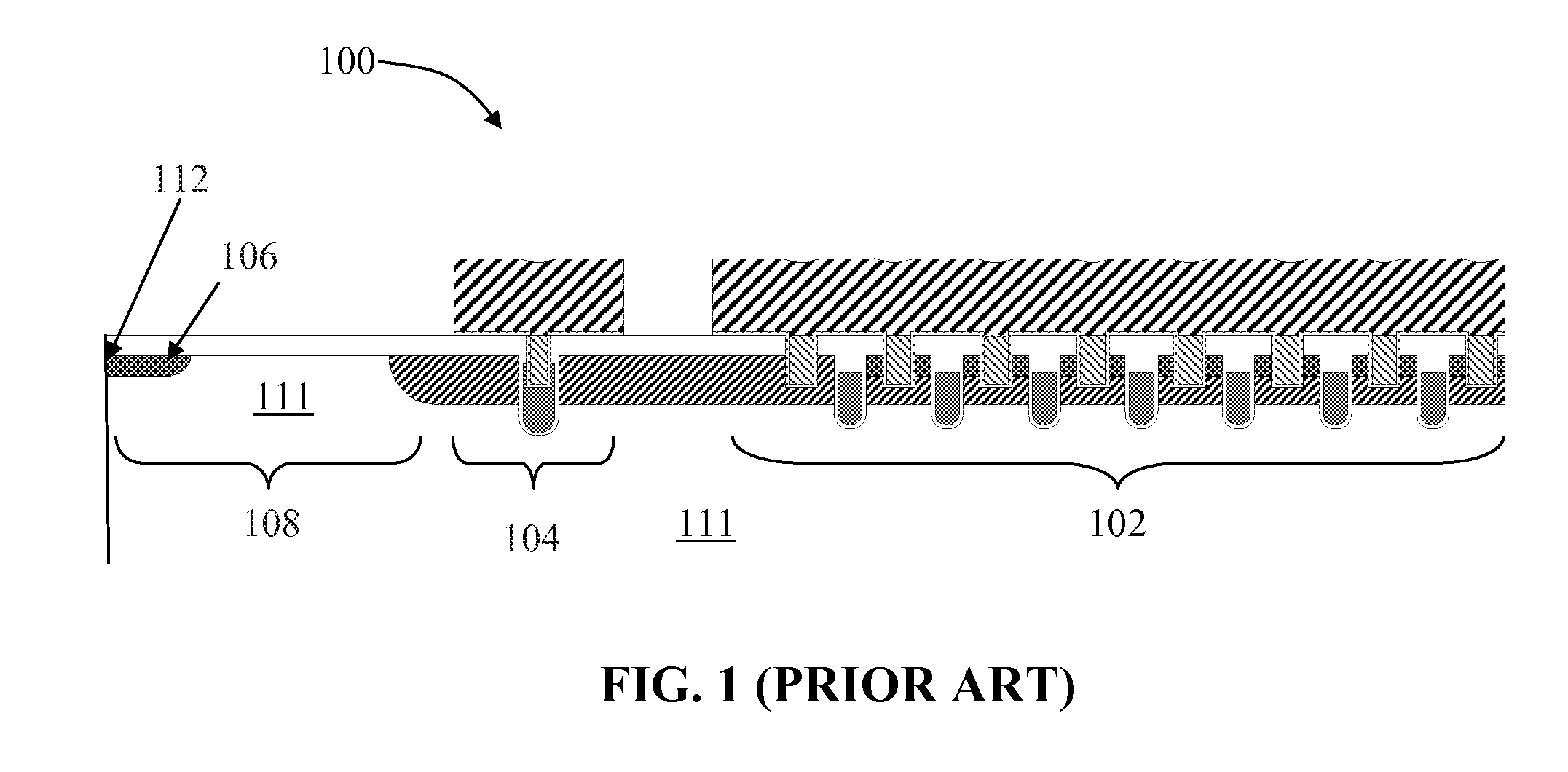
However, a conventional method of making such a trench DMOS field effect transistor requires a five to six masks process that is expensive and time consuming.

Method used


Image

  • Method for making dual gate oxide trench MOSFET with channel stop using three or four masks process
  • Method for making dual gate oxide trench MOSFET with channel stop using three or four masks process
  • Method for making dual gate oxide trench MOSFET with channel stop using three or four masks process

Examples


embodiments

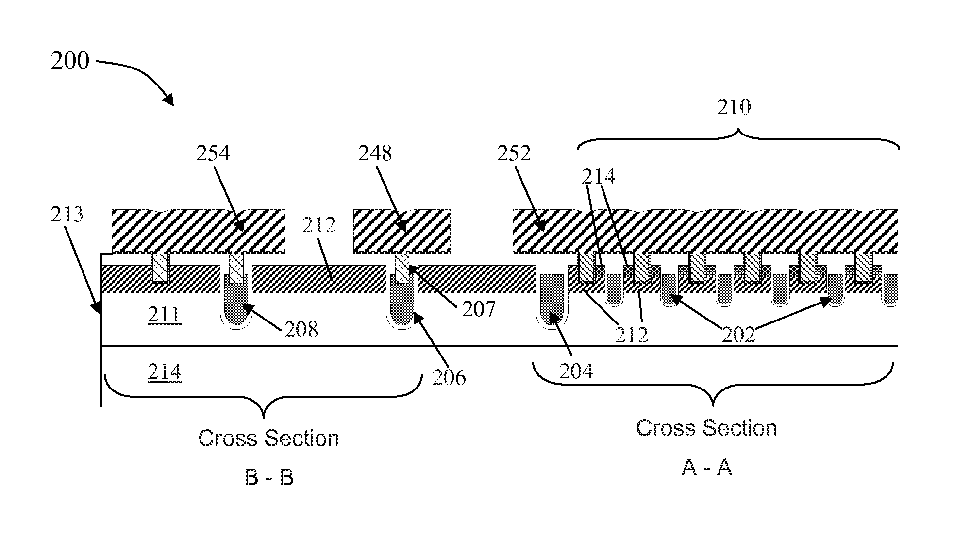
[0025]In embodiments of the present invention, the existing junction termination in a conventional trench MOSFET can be replaced with a thick gate oxide in the gate runner area to terminate the active cell area, which eliminates junction termination breakdown, improves the UIS capability, and saves space occupied by the junction termination because the oxide requires much less space than a conventional junction termination. In addition, reverse recovery is improved by confining the built-in body diode to the active area.

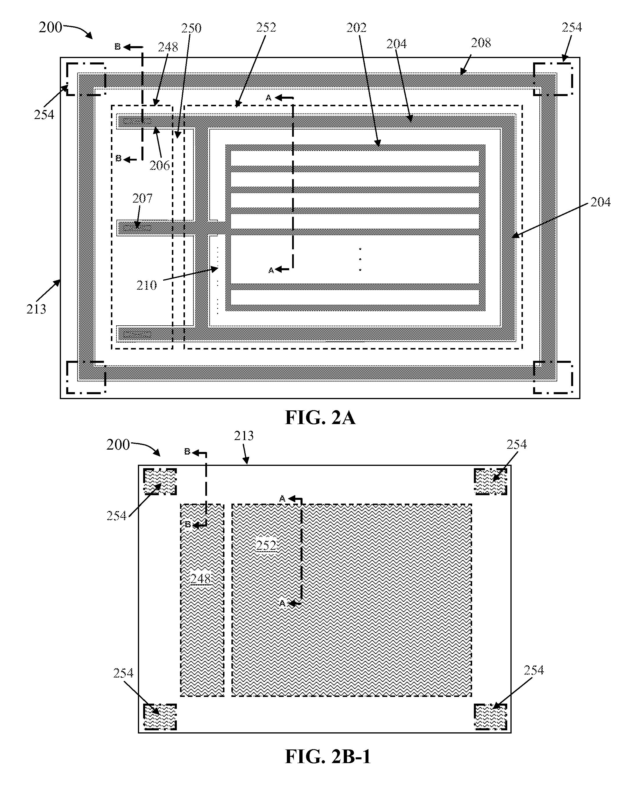
[0026]FIG. 2A is a top view of a layout of the dual gate oxide trench MOSFET 200 of a first embodiment of the present invention and FIG. 2B-2 is a cross-sectional view of the dual gate terminated trench MOSFET 200 along the lines A-A and B-B. The method for making the oxide termination trench MOSFET 200 only requires four masks: a trench mask, a gate oxide mask, a contact mask and a metal mask, which is described later in FIGS. 4A-4R.

[0027]As shown in FIGS. 2A and 2B...


PUM


Abstract

A semiconductor device and fabrication methods are disclosed. The device includes a plurality of gate electrodes formed in trenches located in an active region of a semiconductor substrate. A first gate runner is formed in the substrate and electrically connected to the gate electrodes, wherein the first gate runner surrounds the active region. A second gate runner is connected to the first gate runner and located between the active region and a termination region. A termination structure surrounds the first and second gate runners and the active region. The termination structure includes a conductive material in an insulator-lined trench in the substrate, wherein the termination structure is electrically shorted to a source or body layer of the substrate thereby forming a channel stop for the device.

Description

CLAIM OF PRIORITY[0001]This application is a continuation-in-part of and claims the priority benefit of commonly-assigned U.S. patent application Ser. No. 12 / 731,112, filed Mar. 24, 2010 to Sik Lui et al. entitled “OXIDE TERMINATED TRENCH MOSFET WITH THREE OR FOUR MASKS”, the entire disclosures of which are incorporated by reference herein.FIELD OF THE INVENTION[0002]This invention generally relates trench metal oxide semiconductor field effect transistors (MOSFETS and more particularly to oxide terminated trench MOSFETs and a method of forming the devices with three or four masks.BACKGROUND OF THE INVENTION[0003]A DMOS (Double diffused MOS) transistor is a type of MOSFET (Metal Oxide Semiconductor Field Effect Transistor) that uses two sequential diffusion steps aligned to the same edge to form the channel region of the transistor. DMOS transistors are often high current devices for low and high voltages, used either as discrete transistors or as components in power integrated circ...

Claims


Application Information

Patent Timeline
Patent Type & Authority Patents(United States)
IPC IPC(8): H01L21/336H01L21/20H01L21/425H01L21/8249H01L29/66
CPCH01L29/407H01L29/7813H01L29/66727H01L29/66734H01L29/7811H01L29/0638H01L29/0653H01L29/0878H01L29/41766H01L29/456H01L29/4236
Inventor TAI, SUNG-SHANLUI, SIKWANG, XIAOBIN
Owner ALPHA & OMEGA SEMICON INC
Learn More