
Optical phase modulation circuit and optical phase modulation method

a phase modulator and optical phase technology, applied in the direction of optics, instruments, electrical equipment, etc., can solve the problems of large power consumption of the drive circuit of the linbo3 phase modulator using a progressive wave type electrode, ineffective optical work of the electric field generated by the drive signal, and large modulation band restriction, etc., to achieve high-speed operation without increasing power consumption

Inactive Publication Date: 2013-07-11
NEC CORP
View PDF5 Cites 16 Cited by
  • Summary
  • Abstract
  • Description
  • Claims
  • Application Information

AI Technical Summary

Benefits of technology

The invention provides an optical phase modulation circuit and method that can operate at high speeds without increasing power consumption.

Problems solved by technology

However, since the speed at which the signal (microwave) for driving the modulator propagates through the electrode attached to the component of the modulator is different from the speed at which the optical signal propagates through the optical waveguide, the electric field generated by the drive signal does not effectively work on the optical signal and the modulation band is thereby restricted.
As a result, the power consumption of the drive circuit of the LiNbO3 phase modulator using a progressive wave type electrode is large.
In addition, it is very difficult to realize a wide-band drive circuit that can operate at high speed with a large output amplitude of 5V or larger in the first place.
However, on the other hand, it becomes very difficult to make the transmission speed of the microwave, which serves as the modulator drive signal, and that of the light equal to each other as described above, and thus restricting the modulation band.

Method used


Image

  • Optical phase modulation circuit and optical phase modulation method
  • Optical phase modulation circuit and optical phase modulation method
  • Optical phase modulation circuit and optical phase modulation method

Examples


first exemplary embodiment

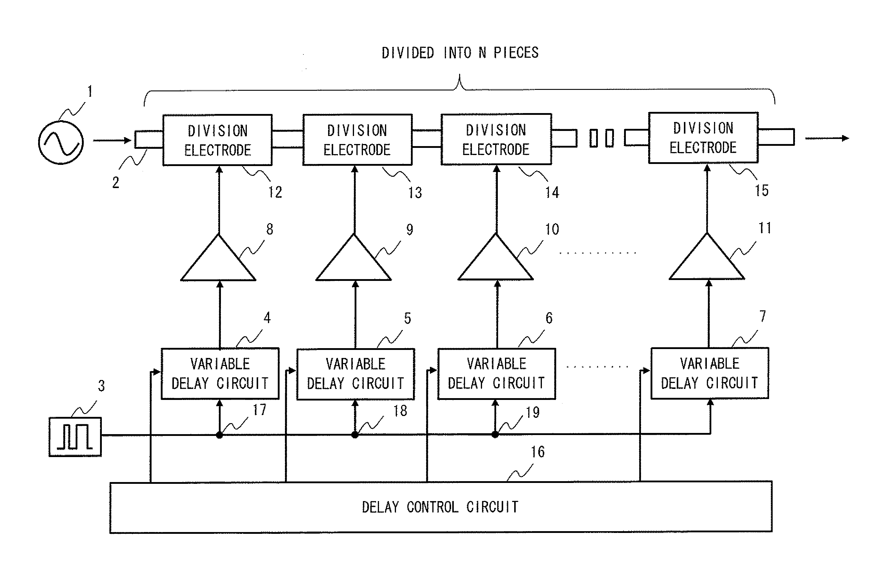
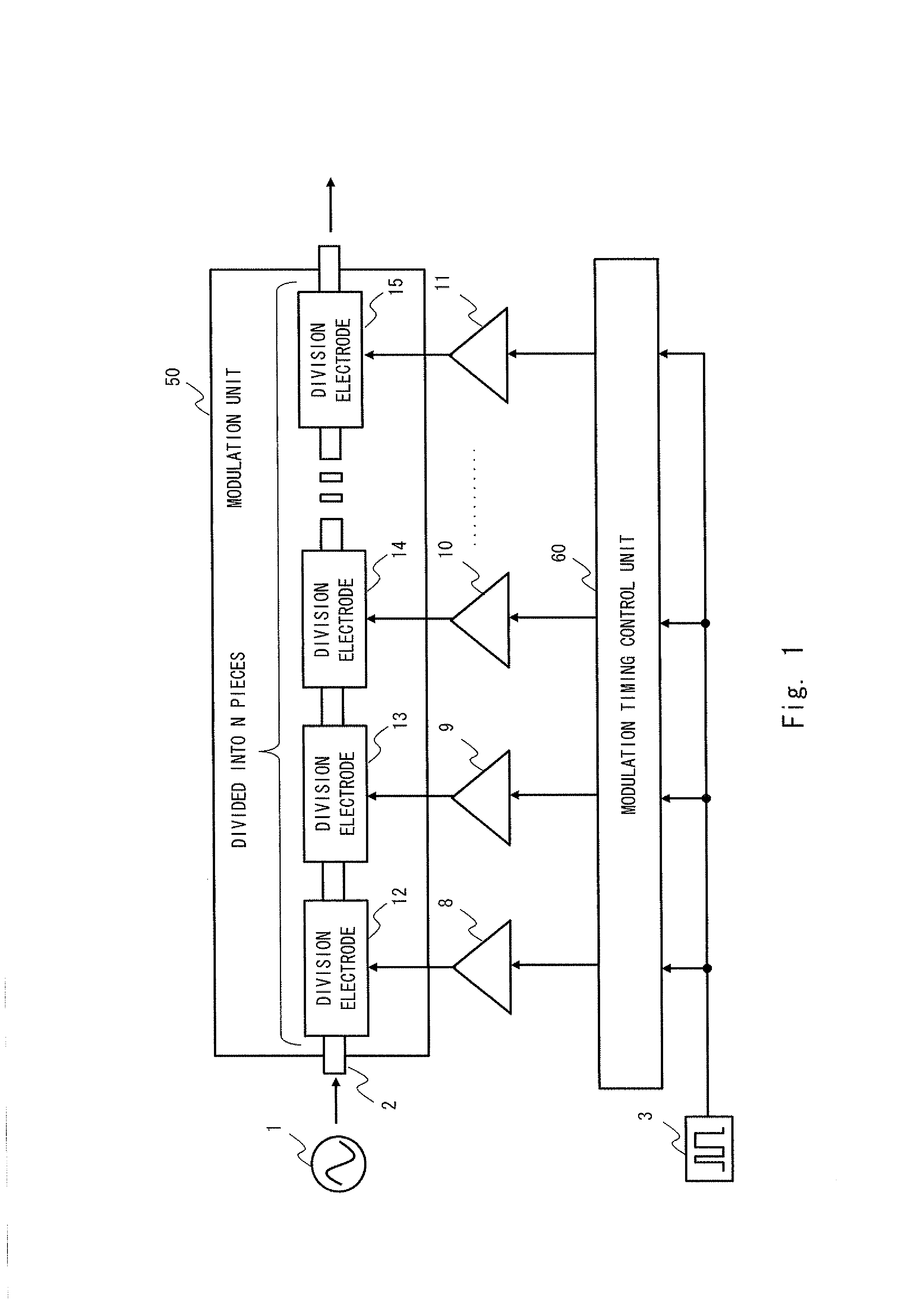
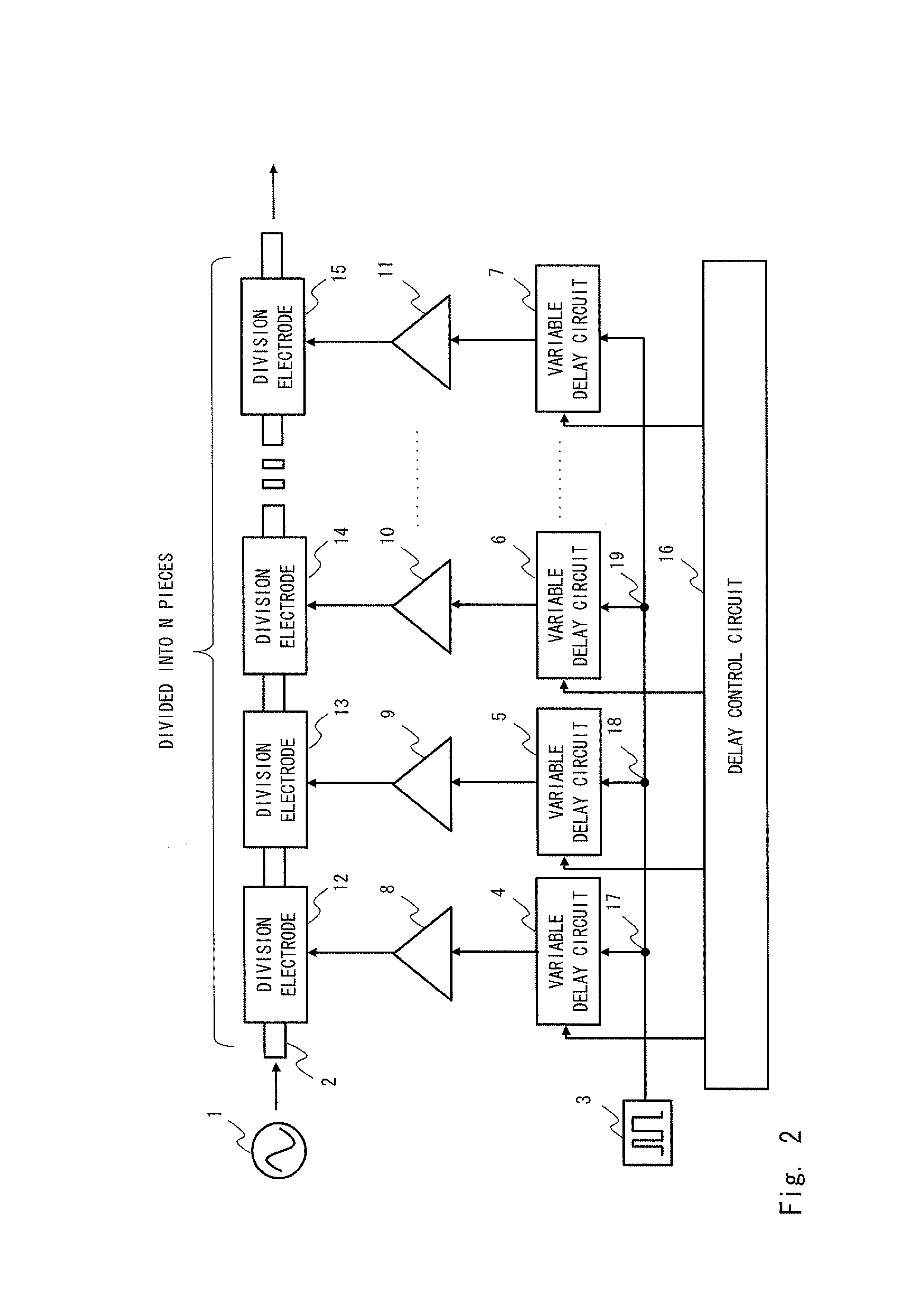
[0029]Exemplary embodiments according to the present invention are explained hereinafter with reference to the drawings. A configuration example of an optical phase modulation circuit according to a first exemplary embodiment of the present invention is explained with reference to FIG. 1. The optical phase modulation circuit includes an optical signal source 1, a signal source 3, drive circuits 8 to 11, and a modulation timing control unit 60. Further, a modulation unit 50 includes division electrodes 12 to 15 and an optical waveguide 2.

[0030]The modulation unit 50 modulates the phase of an optical signal output from the optical signal source 1 to the optical waveguide 2. The modulation unit 50 outputs an optical signal whose phase has been modulated. The modulation unit 50 modulates the phase of an optical signal by using the division electrodes 12 to 15. The division electrodes 12 to 15 are disposed in the optical waveguide 2. Further, the division electrodes 12 to 15 are connecte...

second exemplary embodiment

[0056]Next, a configuration example of an optical phase modulation circuit according to a second exemplary embodiment of the present invention is explained with reference to FIG. 8. The optical phase modulation circuit shown in FIG. 8 includes a clock signal source 31, in addition to the components of the optical phase modulation circuit shown in FIG. 2. Further, the variable delay circuit 4 is composed of a variable phase shifter 32 and a D-flip-flop circuit 36. Similarly, the variable delay circuits 5 to 7 are composed of variable phase shifters 33 to 35 and D-flip-flop circuits 37 to 39. The other configuration is similar to that of the optical phase modulation circuit shown in FIG. 1, and therefore its detailed explanation is omitted.

[0057]An operation of the variable delay circuits 4 to 7 is explained hereinafter. The clock signal source 31 outputs a clock signal to the variable phase shifters 32 to 35. Further, the delay control circuit 16 outputs a control signal whose delay ...

third exemplary embodiment

[0060]Next, a configuration example of an optical phase modulation circuit according to a third exemplary embodiment of the present invention is explained with reference to FIG. 9. The optical phase modulation circuit shown in FIG. 9 includes a waveform monitoring circuit 41, in addition to the components of the optical phase modulation circuit shown in FIG. 2. Note that the waveform monitoring circuit 41 may be also incorporated in the optical phase modulation circuit shown in FIG. 8. The other configuration is similar to that shown in FIG. 2, and therefore its detailed explanation is omitted.

[0061]The waveform monitoring circuit 41 monitors the waveform of an optical signal output from the optical waveguide 2 and outputs a monitoring result to the delay control circuit 16. There is a possibility that the waveform of the optical signal output from the optical waveguide 2 is disturbed due to temperature variations, power supply variations, variations resulting from process variation...


PUM

PropertyMeasurementUnit
drive voltageaaaaaaaaaa
phaseaaaaaaaaaa
timeaaaaaaaaaa

Abstract

To provide an optical phase modulation circuit and an optical phase modulation method capable of achieving a high-speed operation without increasing the power consumption. An optical phase modulation circuit according to the present invention includes an optical modulation unit 50 that includes a plurality of division electrodes 12 to 15 connected in tandem and generates a modulation signal by summing up optical signals modulated by using respective division electrodes, drive circuits 8 to 11 that drive the plurality of division electrodes, and a modulation timing control unit 60 that controls timings at which the optical signals are modulated in the plurality of division electrodes 12 to 15, by controlling an operation timing of the drive circuits 8 to 11.

Description

TECHNICAL FIELD[0001]The present invention relates to an optical phase modulation circuit and an optical phase modulation method, in particular to an optical phase modulation circuit used in coherent light communication and an optical phase modulation method used in that optical phase modulation circuit.BACKGROUND ART[0002]As the demand for broadband multimedia communication such as the Internet and video image distributions has increased explosively, the introduction of high-density multiple-wavelength optical fiber communication systems having a larger capacity and higher reliability for a longer distance is in progress in trunk-line and metro networks. Further, even in subscriber's networks, the optical fiber access service is becoming widespread rapidly. In such communication systems using optical fibers, it is important to reduce the cost for installing optical fibers, which serve as optical transmission paths, and increase the transmission band use efficiency per optical fiber...

Claims


Application Information

Patent Timeline
Patent Type & Authority Applications(United States)
IPC IPC(8): G02F1/01H04B10/556
CPCH04B10/5561G02F1/0121G02F2201/16G02F1/0356G02F1/0327
Inventor NOGUCHI, HIDEMI
Owner NEC CORP
Learn More