Semiconductor Device Package with Slanting Structures

a technology of slant structure and semiconductor device, which is applied in the direction of semiconductor device details, semiconductor/solid-state device details, electrical apparatus, etc., can solve the problems of difficult hand-soldering of qfn package and usually more expensive, and achieve the effect of improving package form factor and reducing package body thickness

Inactive Publication Date: 2013-07-18
KING DRAGON INT
View PDF4 Cites 8 Cited by
  • Summary
  • Abstract
  • Description
  • Claims
  • Application Information

AI Technical Summary

Benefits of technology

[0009]One object of the present invention is to provide a semiconductor device package with slanting structures, thereby improving the package form fa

Problems solved by technology

It is usually more expensive due to its construction, and can be used for microwav

Method used


Image

  • Semiconductor Device Package with Slanting Structures
  • Semiconductor Device Package with Slanting Structures
  • Semiconductor Device Package with Slanting Structures

Examples


Embodiment Construction

[0016]The present invention will now be described with the preferred embodiments and aspects and these descriptions interpret structure and procedures of the present invention only for illustrating but not for limiting the Claims of the present invention. Therefore, except the preferred embodiments in the specification, the present invention may also be widely used in other embodiments.

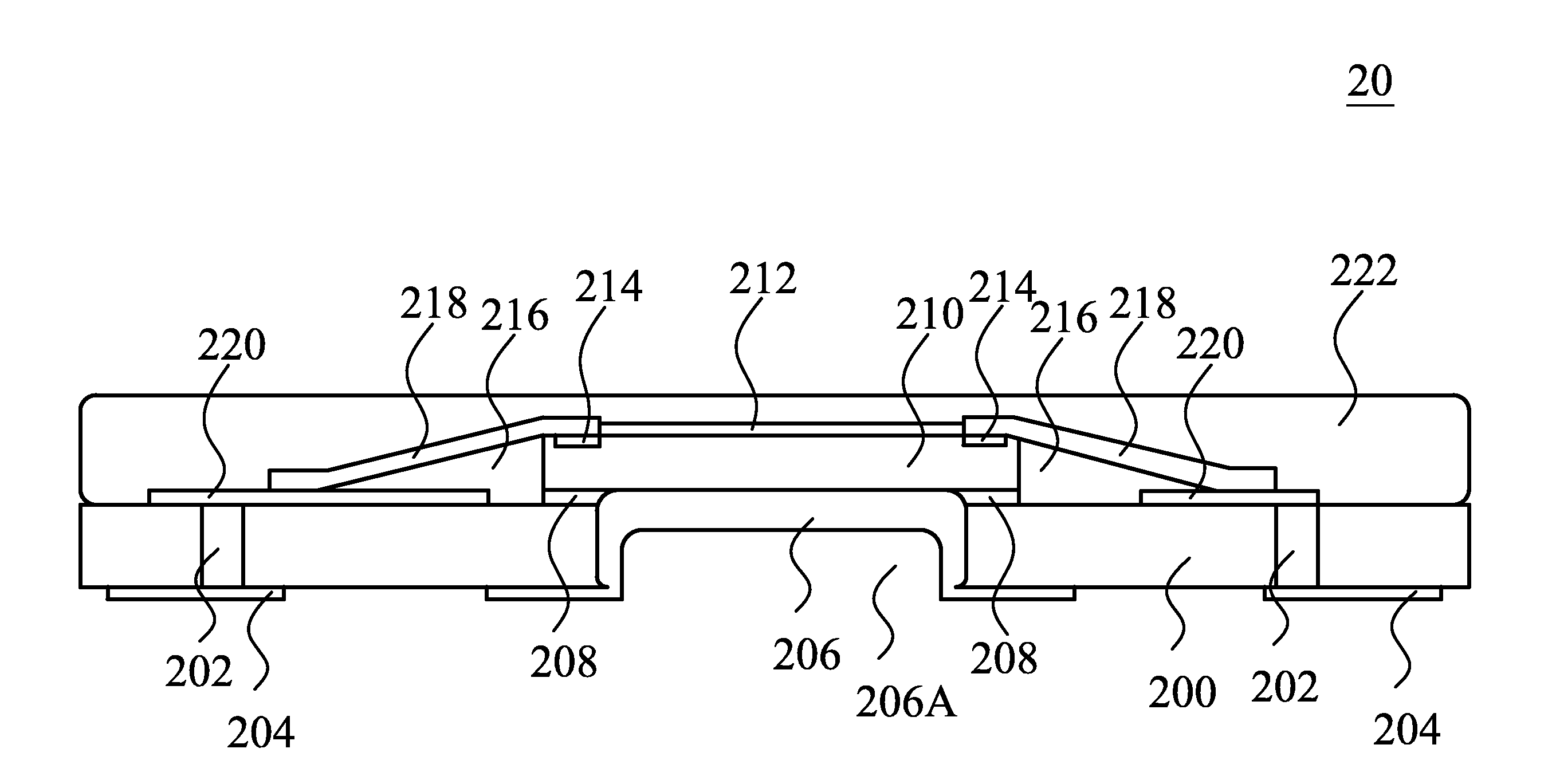
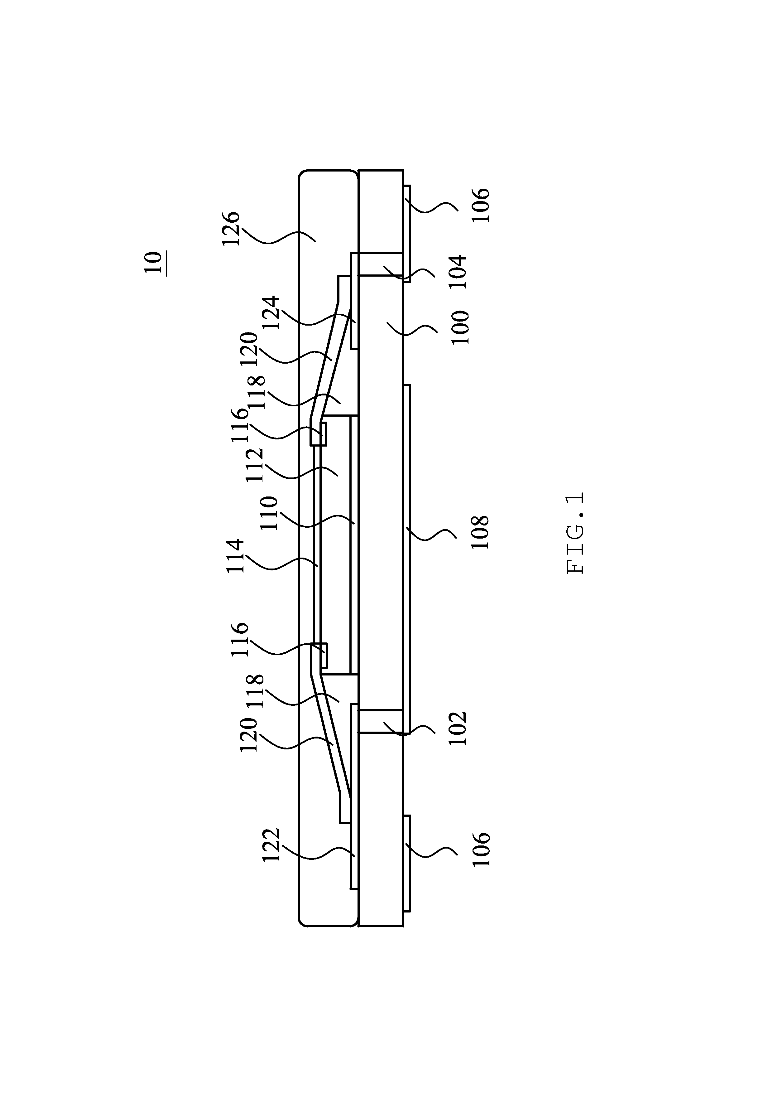
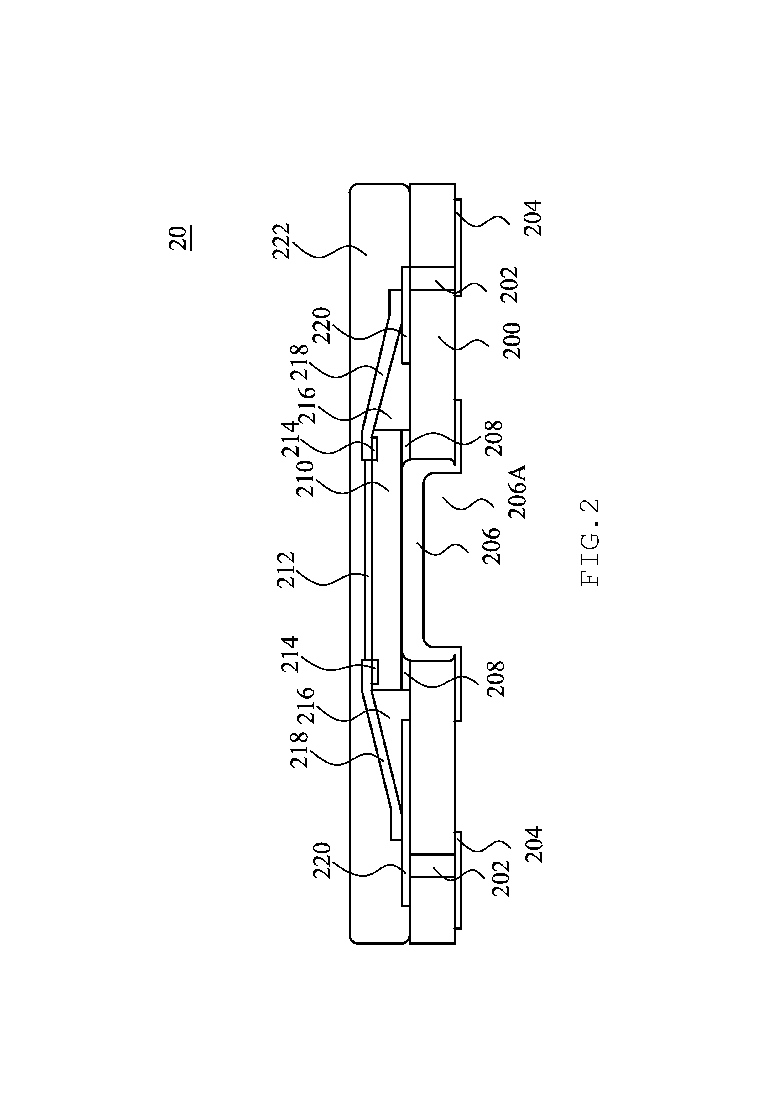
[0017]FIG. 1 is cross-sectional view of a semiconductor device package 10 for QFN (quad-flat no-leads) package. The semiconductor device package 10 has a substrate 100 with predetermined through-holes 102 and 104 formed therein. The material of the substrate 100 may be a metal, glass, ceramic, silicon, plastic, BT(bismaleimide triazine), FR4, FR5 or PI(polyimide) etc. In one embodiment, the thickness of the substrate 100 may be about 40-200 micron-meters. It may be a single or multi-layer (wiring circuit) substrate.

[0018]A die 112 with bonding pads 116 thereon is subsequently adhered on the upper surf...


PUM


Abstract

A semiconductor device package structure includes a substrate with a via contact pad on top surface of the substrate, a terminal pad on bottom surface of the substrate and a conductive through hole through the substrate, wherein the conductive through hole electrically couples the via contact pad and the terminal pad on the substrate; a die having bonding pads thereon, wherein the die is formed on the top surface of the substrate; a slanting structure formed adjacent to at least one side of the die for carrying conductive traces; and a conductive trace formed on upper surface of the slanting structure to offer path between the bonding pads and the via contact pad.

Description

CROSS-REFERENCE[0001]The present application is a continuation-in-part (CIP) application of a pending U.S. application Ser. No. 13 / 348,787, entitled “LED Package with Slanting Structure and Method of the Same”, and filed on Jan. 12, 2012, which is incorporated herein by reference in its entirety.FIELD OF THE INVENTION[0002]The present invention relates to a semiconductor device package, and more particularly to a semiconductor device package with slanting structures formed adjacent to the die.BACKGROUND OF THE INVENTION[0003]In the field of semiconductor devices, the device density is increased and the device dimension is reduced, continuously. The demand for the packaging or interconnecting techniques in such high density devices is also increased to fit the situation mentioned above. Flat no-leads packages such as QFN (quad-flat no-leads) and DFN (dual-flat no-leads) physically and electrically connect integrated circuits to printed circuit boards. Flat no-leads, also known as Mic...

Claims


Application Information

Patent Timeline
IPC IPC(8): H01L23/48
CPCH01L2224/24998H01L23/49827H01L24/24H01L24/32H01L2224/32225H01L24/25H01L24/82H01L2224/2518H01L2224/73267H01L2224/83855H01L2224/92244H01L2924/15151H01L23/3121H01L23/3677H01L2224/24226H01L2924/15747H01L2924/12042H01L2924/181H01L2924/00H01L2924/00012
Inventor YANG, WEN KUN
Owner KING DRAGON INT
Why Eureka
Try Eureka