Test system and test method for pcba

a technology of printed circuit board and test system, which is applied in the field of test system, can solve the problems of damage to the modules/components, increased manufacturing cost, and additional cost for manufacturers to perform testing with actual modules/components

Inactive Publication Date: 2013-07-18
WISTRON CORP
View PDF8 Cites 10 Cited by
  • Summary
  • Abstract
  • Description
  • Claims
  • Application Information

AI Technical Summary

Benefits of technology

This patent describes a test system and method for testing a printed circuit board assembly (PCBA) that includes a printed circuit board (PCB) with various traces and a CPU socket and memory module slots. The test system includes a CPU interposer board and memory module interposer boards that are inserted into the CPU socket and memory module slots, respectively. The test loop is formed by coupling the PCB's traces to the CPU interposer board to form a loop from the test point to the CPU interposer board, and then coupling the memory module interposer boards to the CPU interposer board to form a loop from the memory module slots to the test point. The test system determines if the test loop is normal or not based on a reflectometry result of a test signal provided through the test point. The technical effects of this test system include improved efficiency and accuracy in testing PBCAs.

Problems solved by technology

In motherboard manufacturing processes, various components disposed on a motherboard need to be tested in advance, to avoid generating problems in production, thereby causing additional costs for manufacturers.
However, a higher manufacturing cost is required to perform testing with the actual modules / components.
Furthermore, repeatedly plugging and pulling the modules / components will easily cause damage to the modules / components.
When the module / component is operating at a critical point of failure, instability will occur in the test.
Therefore, a test engineer needs to further analyze whether the module / component is damaged or the motherboard is abnormal, thus increasing test time and test costs.
However, it cannot test whether connections between the slot 20 and the other modules / components of the motherboard 1 are normal.

Method used


Image

  • Test system and test method for pcba
  • Test system and test method for pcba
  • Test system and test method for pcba

Examples


Embodiment Construction

[0020]The following description is of the best-contemplated mode of carrying out the invention. This description is made for the purpose of illustrating the general principles of the invention and should not be taken in a limiting sense. The scope of the invention is best determined by reference to the appended claims.

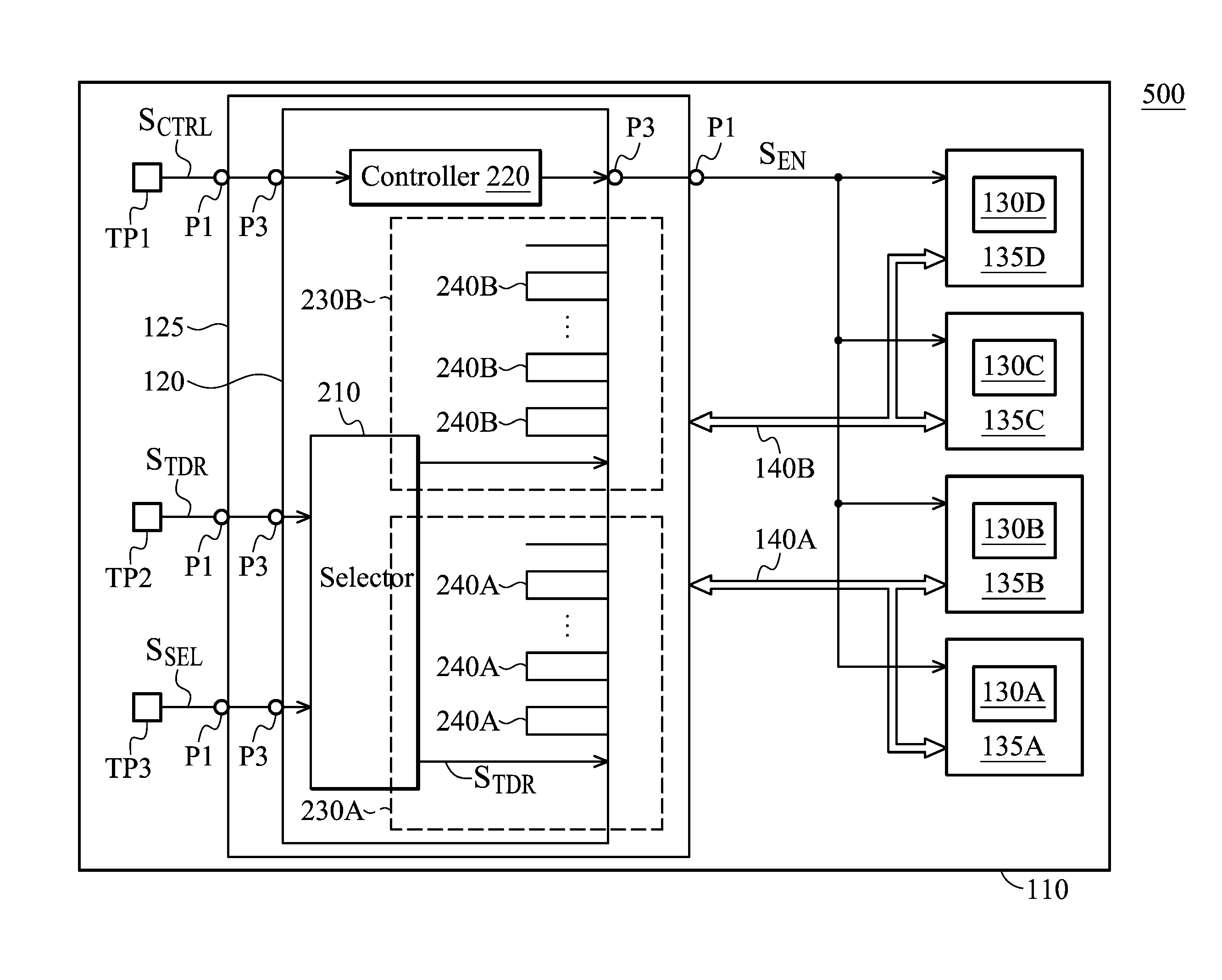
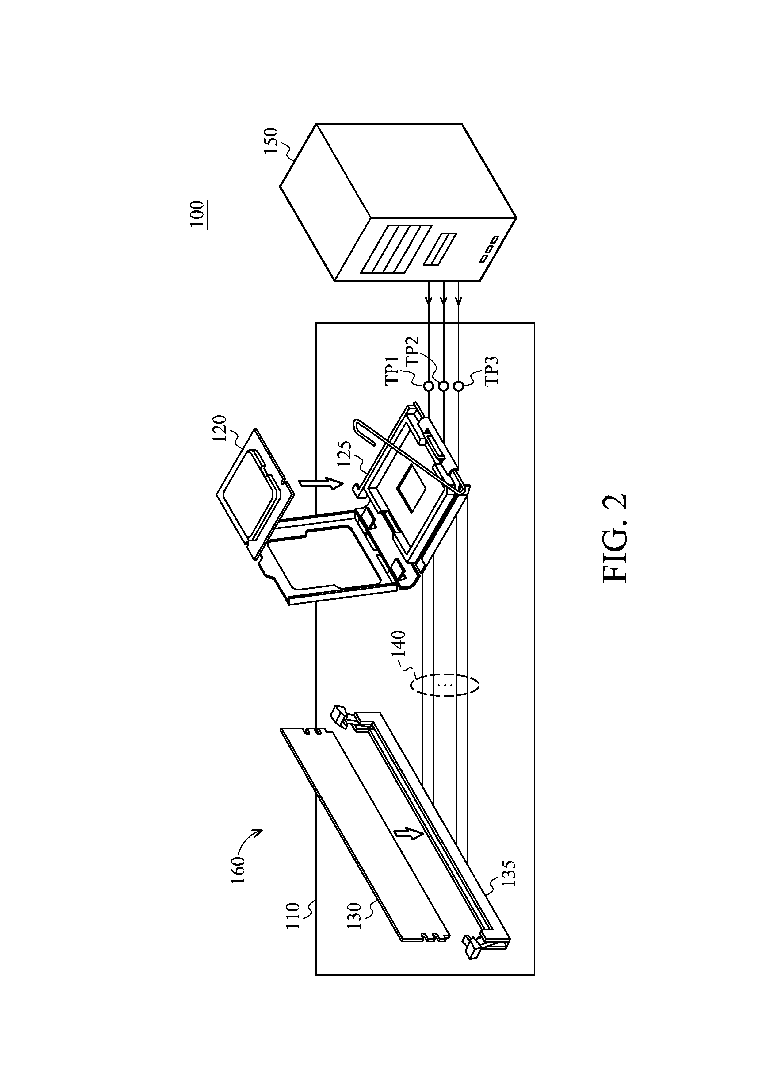
[0021]FIG. 2 shows a test system 100 according to an embodiment of the invention. The test system 100 comprises a printed circuit board assembly (PCBA) 160 to be tested, a central processing unit (CPU) interposer board 120, a memory module interposer board 130 and automatic test equipment (ATE) 150, wherein the PCBA 160 comprises a printed circuit board (PCB) 110, a CPU socket 125 and a memory module slot 135. The CPU socket 125 and the memory module slot 135 are disposed on the PCB 110, wherein the CPU socket 125 is electrically coupled to the memory module slot 135 via a plurality of traces 140 of the PCB 110. Furthermore, the PCB 110 further comprises the test point...


PUM


Abstract

A test system is provided. A printed circuit board (PCB) includes a plurality of traces and at least one test point. A central processing unit (CPU) socket including a plurality of first pins and a memory module slot including a plurality of second pins are disposed on the PCB. Each of the second pins is coupled to the corresponding first pin of the CPU socket via the corresponding trace. A CPU interposer board is inserted into the CPU socket, and a memory interposer board is inserted into the memory module slot. The traces form a test loop via the CPU interposer board and the memory interposer board. When an automatic test equipment (ATE) provides a test signal to the test loop via the test point, the ATE determines whether the test loop is normal according to a reflectometry result of the test signal.

Description

CROSS REFERENCE TO RELATED APPLICATIONS[0001]This Application claims priority of Taiwan Patent Application No. 101101339, filed on Jan. 13, 2012, the entirety of which is incorporated by reference herein.BACKGROUND OF THE INVENTION[0002]1. Field of the Invention[0003]The invention relates to a test system, and more particularly to a test system for a printed circuit board assembly (PCBA).[0004]2. Description of the Related Art[0005]In motherboard manufacturing processes, various components disposed on a motherboard need to be tested in advance, to avoid generating problems in production, thereby causing additional costs for manufacturers.[0006]In general, when testing whether a slot or a connector of a motherboard is normal, e.g. whether solder is empty, or there is an open circuit, or short circuit or there are other abnormal states occurring between the slot and the motherboard, a memory module, an interface card or a central processing unit (CPU) that is a module / component actual...

Claims


Application Information

Patent Timeline
Patent Type & Authority Applications(United States)
IPC IPC(8): G01R31/28
CPCG01R31/2812G01R31/11
Inventor LIU, KUAN-LINPENG, KUO-JUNG
Owner WISTRON CORP
Why Eureka
Try Eureka