Optical modulator

a technology of optical modulator and light intensity ratio, which is applied in the field of optical modulator, can solve the problems of weak resistance to bias drift, increase in the size of the entire element, and easy influence of means, and achieve the effect of easy adjustment of light intensity ratio in optical modulator, stable yield and miniaturization or integration of elements

Active Publication Date: 2013-08-01
SUMITOMO OSAKA CEMENT CO LTD +1
View PDF2 Cites 14 Cited by
  • Summary
  • Abstract
  • Description
  • Claims
  • Application Information

AI Technical Summary

Benefits of technology

[0030]According to the first aspect of the present invention, an optical modulation unit is provided which includes a Mach-Zehnder type optical waveguide and a modulation electrode for modulating light waves propagating through the Mach-Zehnder type optical waveguide. The plurality of optical modulation units is disposed in parallel on the same substrate. One input waveguide branches off to be connected to the Mach-Zehnder type optical waveguide of each optical modulation unit, and an entire optical waveguide is formed such that outputs from the Mach-Zehnder type optical waveguides are combined and output through one output waveguide. A modulation signal with a same intensity is applied to a modulation electrode of each optical modulation unit. In at least some of the optical modulation units, mechanical structures including the modulation electrodes of the optical modulation unit are configured such that an amplitude value of an optical output modulated by the modulation signal of the optical modulation unit is ½n (n is a natural number) of a maximum amplitude value in other optical modulation units at which an amplitude value of the optical output modulated by the modulation signals is the greatest. Therefore, it is possible to easily adjust the light intensity ratio in the optical modulator. In particular, a light intensity adjusting mechanism such as an attenuator, adjusting the branching ratio in a branching portion of an optical waveguide, adjusting the amplitude ratio of modulation signals in an external circuit, and the like are not necessary unlike in the related art. For this reason, since there needs no addition of a new component, miniaturization or integration of elements can be realized. As a result, since it becomes less influenced by manufacturing variations, a stable yield can be expected. In addition, since the amplitude of an RF signal input to the optical modulator can be constant, an adjustment point on the input signal is not necessary.
[0031]According to the second aspect of the present invention, since the mechanical structure of the optical modulation unit is configured such that a length of the modulation electrode is {cos−1(1−21−n)}/π (n is a natural number) compared with those of other optical modulation units, it is possible to easily adjust the light intensity ratio just by adjusting the shape of the modulation electrode at the time of manufacturing.
[0032]According to the third aspect of the present invention, since the mechanical structures of the optical modulation unit are configured by adjusting a depth of a ridge that forms an optical waveguide, a width of a signal electrode that forms a modulation electrode, a gap between a signal electrode and a ground electrode, positional relationship between a modulation electrode and an optical waveguide, a width of an optical waveguide, a polarization inversion structure, a thickness of a substrate, or an dielectric constant under a substrate for each optical modulation uni...

Problems solved by technology

However, these cause an increase in the size of the entire element.
However, there are disadvantages in that the means is easily influenced by manufacturing deviations and the like.
As a result, resistance to the bias drift becomes weak.
In the case of the above (2), however, a problem of the selection of dither signal frequencies occurs.
Due to such frequency limit...

Method used


Image

  • Optical modulator
  • Optical modulator
  • Optical modulator

Examples


Embodiment Construction

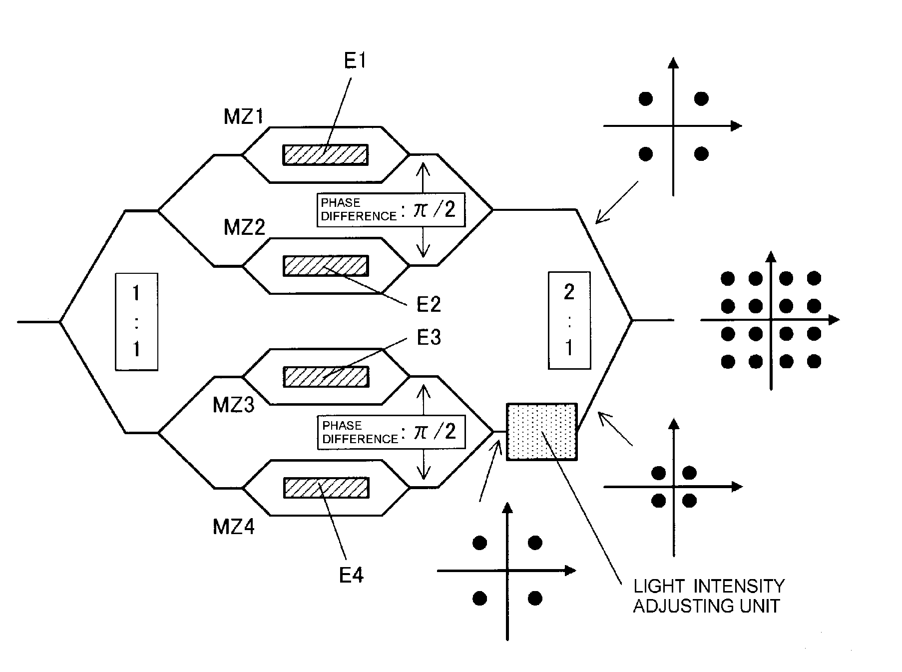
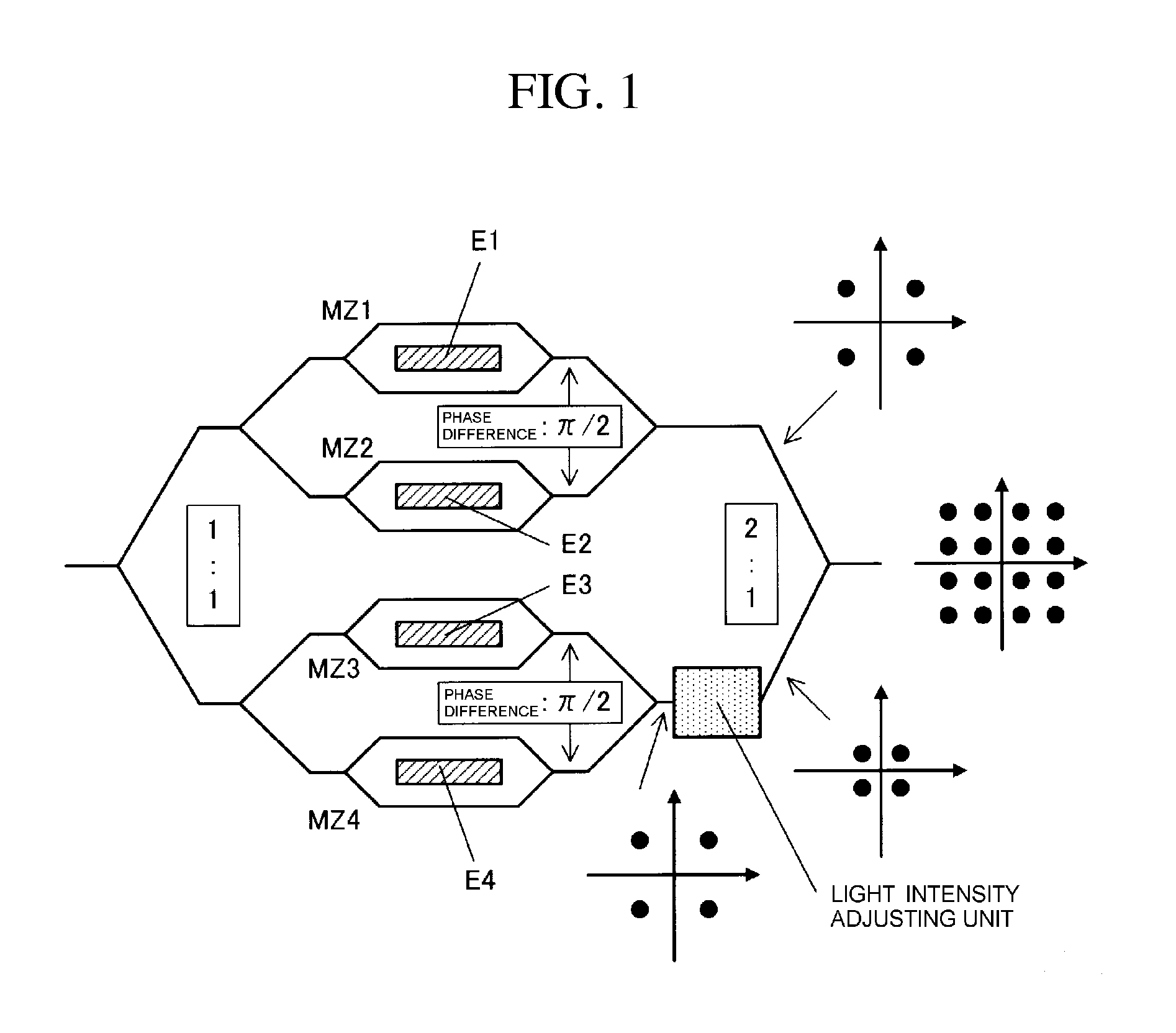
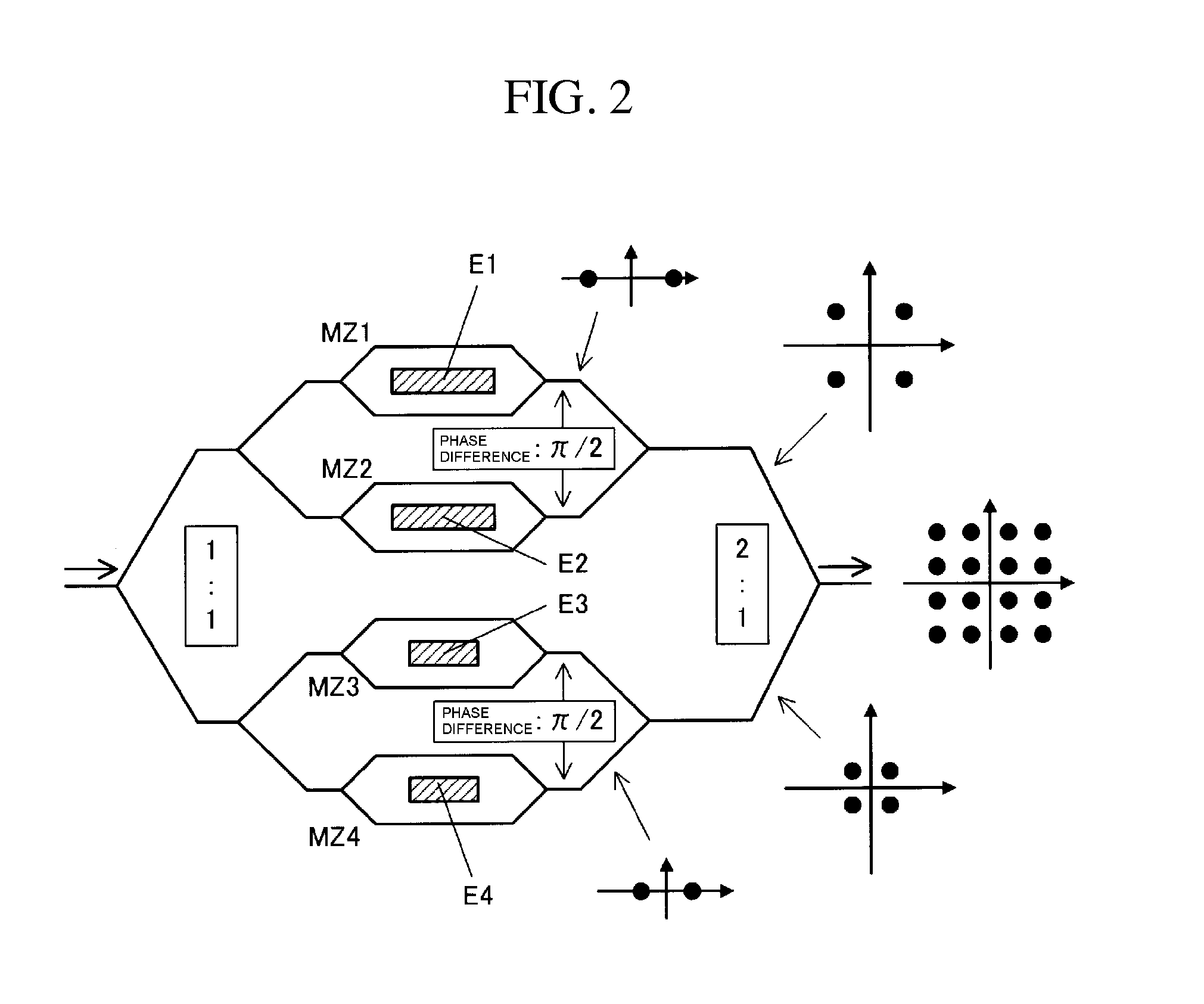
[0051]Hereinafter, an optical modulator of the present invention will be described in detail. As shown in FIG. 2, the optical modulator of the present invention includes optical modulation units having Mach-Zehnder type optical waveguides (MZ1 to MZ4) and modulation electrodes (E1 to E4) for modulating light waves propagating through the Mach-Zehnder type optical waveguides. In the optical modulator, a plurality of optical modulation units are disposed in parallel on the same substrate, and one input waveguide branches off to be connected to the Mach-Zehnder type optical waveguide of each optical modulation unit and the entire optical waveguide is formed such that outputs from the Mach-Zehnder type optical waveguides are combined and output through one output waveguide. A modulation signal with the same intensity is applied to the modulation electrode of each optical modulation unit. In at least some optical modulation units, mechanical structures including the modulation electrodes...


PUM


Abstract

The optical modulator includes optical modulation units. The plurality of optical modulation units is disposed in parallel on the same substrate. One input waveguide branches off to be connected to the Mach-Zehnder type optical waveguide of each optical modulation unit, and an entire optical waveguide is formed such that outputs from the Mach-Zehnder type optical waveguides are combined and output through one output waveguide. A modulation signal with the same intensity is applied to a modulation electrode of each optical modulation unit. In at least some of the optical modulation units, mechanical structures including the modulation electrodes of the optical modulation units are configured such that an amplitude value of an optical output modulated by the modulation signal of the optical modulation unit is ½n (n is a natural number) of a maximum amplitude value in other optical modulation units.

Description

TECHNICAL FIELD[0001]Priority is hereby claimed to Japan Patent Application No. 2012-017673 filed on Jan. 31, 2012, and such priority application is hereby incorporated by reference herein, in its entirety. The present invention relates to an optical modulator and in particular, to an optical modulator operable in a quadrature amplitude modulation (QAM) format (including a multiplexing method using polarization multiplexing and the like) of 2n values (n is a natural number).BACKGROUND ART[0002]In optical communication technology, in order to increase the information density, an optical modulator based on a multi-level modulation scheme of 16-QAM or higher is under development.[0003]As shown in PTL 1 or PTL 2, in a modulator having a configuration in which quadrature phase-shift keying (QPSK) structures are disposed in a nested structure, it is possible to generate an amplitude-shift keying (ASK) signal or a QAM signal by generating binary phase-shift keying (BPSK) signals, which are...

Claims


Application Information

Patent Timeline
IPC IPC(8): G02F1/035
CPCH04B10/5053H04B10/541G02F2201/18G02F1/0123G02F1/225G02F1/035
Inventor HOSOKAWA, YOUICHIHIGUMA, KAORUKAWANISHI, TETSUYAKANNO, ATSUSHI
Owner SUMITOMO OSAKA CEMENT CO LTD
Why Eureka
Try Eureka