

Pre-cut wafer applied underfill film on dicing tape
- Summary
- Abstract
- Description
- Claims
- Application Information
AI Technical Summary
Benefits of technology
Problems solved by technology
Method used
Image

Examples
Embodiment Construction
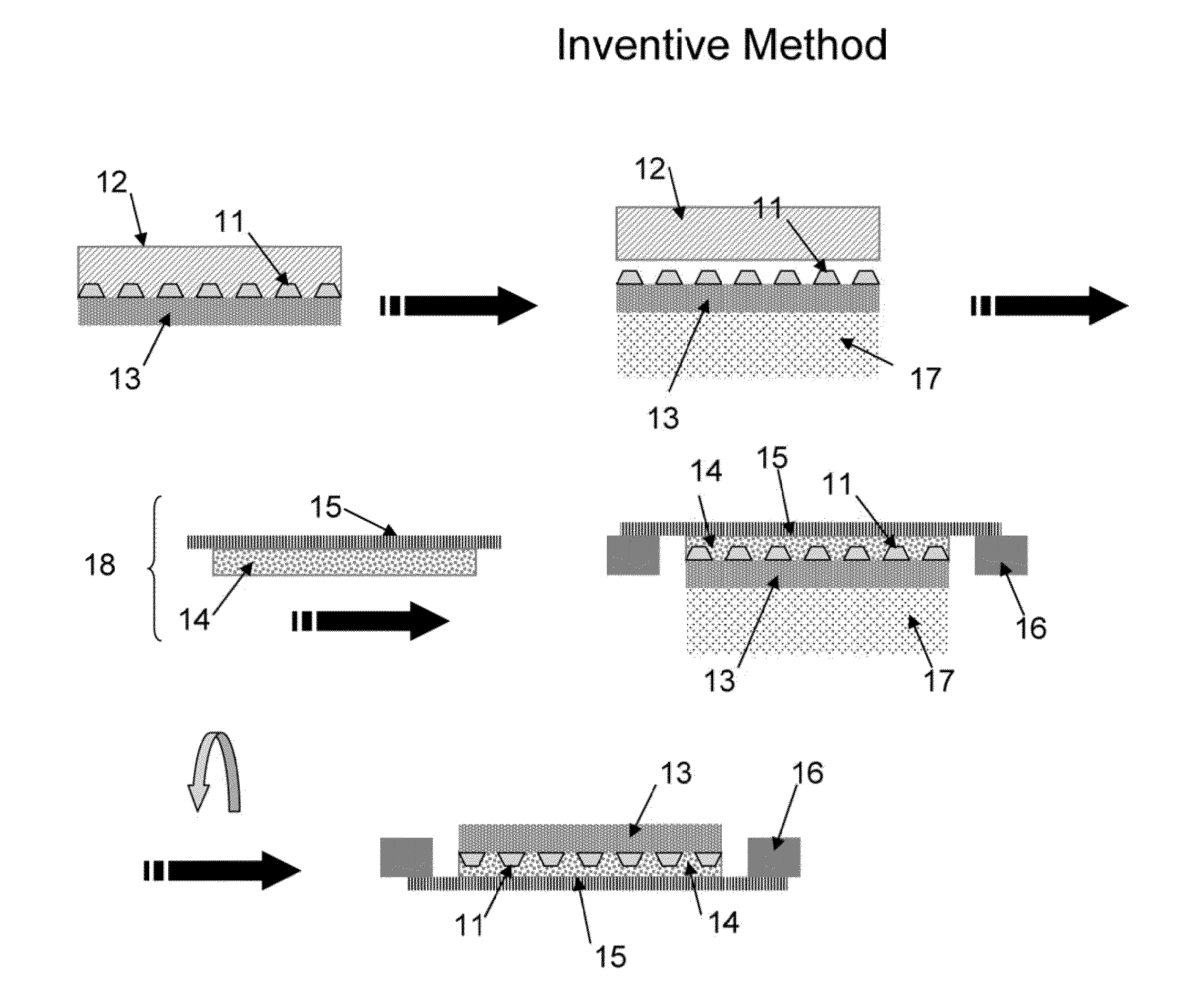
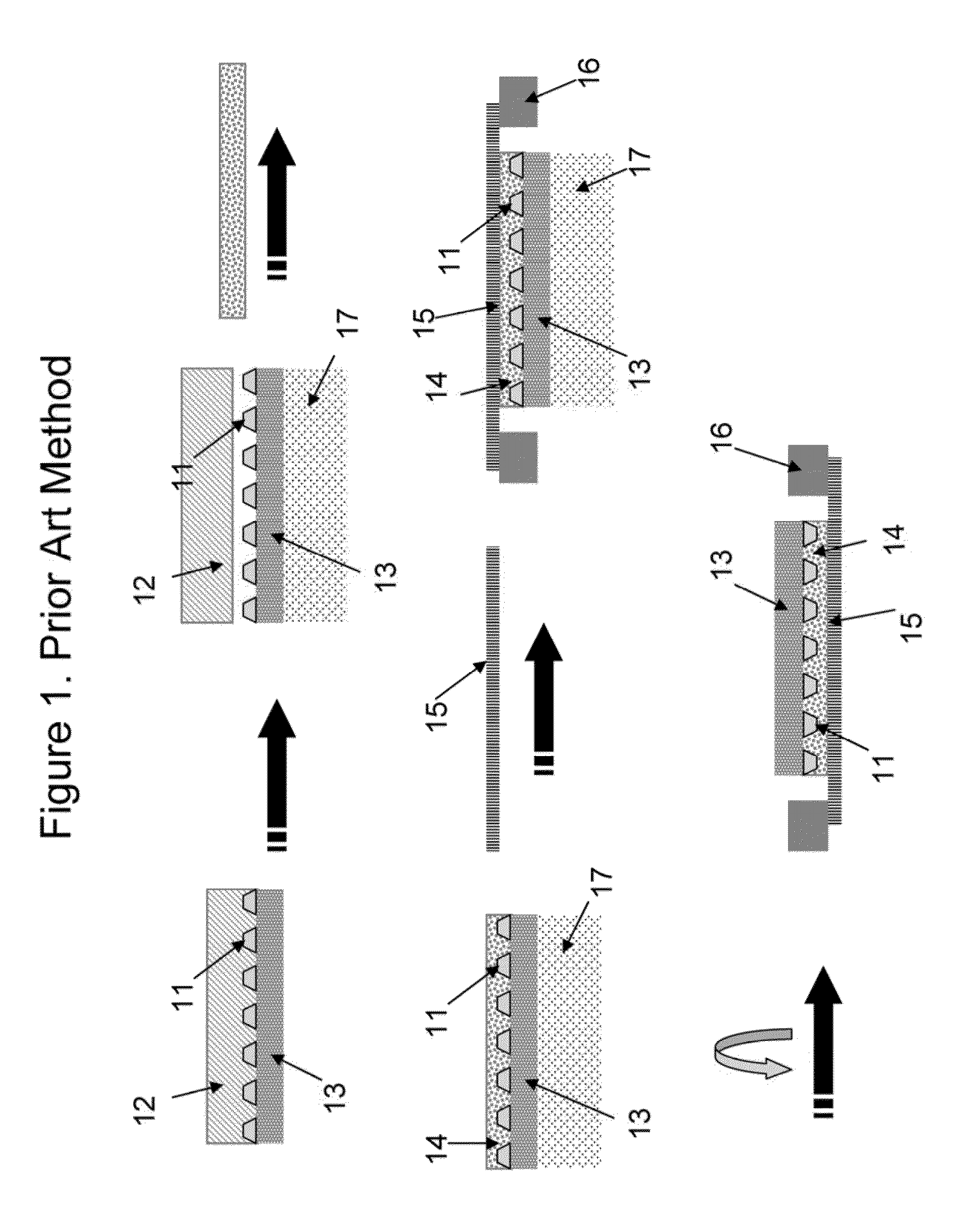
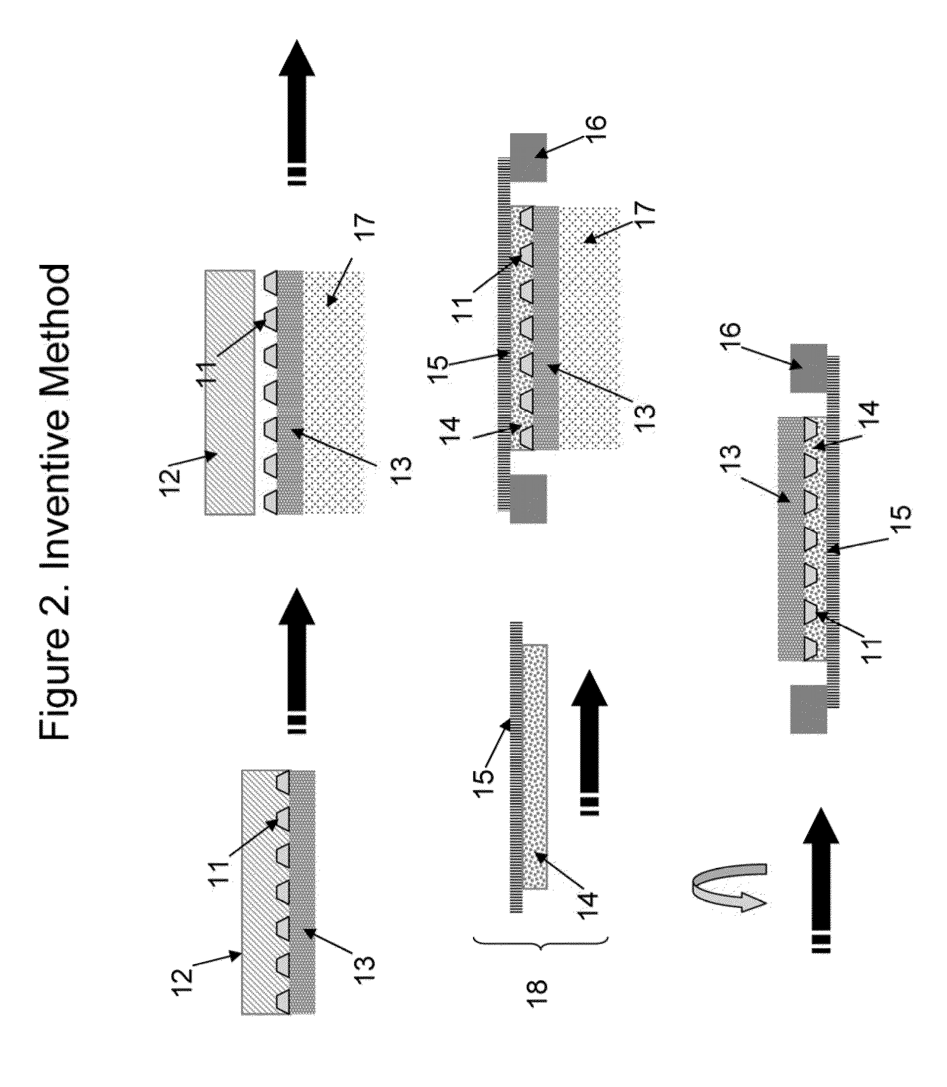
[0010]This invention is a method for the preparation of a semiconductor wafer for dicing. The semiconductor wafer has a plurality of metallic bumps on its active face. The essence of this invention is the use of a dicing tape having an underfill material disposed on one side. The dicing tape / underfill thus supplies the underfill material and the dicing tape in one step. Rather than applying an underfill material to the semiconductor wafer, and in a separate step, mounting the dicing tape over the underfill, the use of the combined dicing tape and underfill eliminates a step in the fabrication process. The assembly of dicing tape, underfill and wafer can be disposed in a dicing frame so that the inactive face of the wafer is oriented upwards, for ease in stealth dicing.
[0011]The wafer is prepared according to known methods from a semiconductor material, typically silicon, gallium arsenide, germanium, or similar compound semiconductor materials. The formation of the plurality of metal...
PUM
 Abstract
Description
Claims
Application Information