
Pre-cut wafer applied underfill film on dicing tape

a technology of dicing tape and thinned silicon, which is applied in the direction of semiconductor devices, semiconductor/solid-state device details, electrical devices, etc., can solve the problems of fragile thinned silicon semiconductor wafers and final device failure, and achieve the effect of avoiding a step in conventional fabrication and facilitating stealth dicing

Active Publication Date: 2016-06-07
HENKEL KGAA
View PDF94 Cites 0 Cited by
  • Summary
  • Abstract
  • Description
  • Claims
  • Application Information

AI Technical Summary

Benefits of technology

This patent describes a way to prepare a semiconductor wafer for cutting without leaving any gaps between the chips. The method involves adding a layer of underfill material to a dicing tape, and then aligning the underfill with the wafer and sticking it on to it. This process helps to prevent cracking and other damage during the cutting process. Additionally, a separation layer can be used between the underfill and the dicing tape to improve the final quality of the chips.

Problems solved by technology

Due to a thermal mismatch that exists between the semiconductor and the substrate, repeated thermal cycling stresses the metallic interconnections, potentially leading to ultimate device failure.
However, thinned silicon semiconductor wafers are fragile, so it is a benefit to utilize processes in semiconductor fabrication that do not threaten the integrity of the wafer as it is being diced into individual semiconductor dies and that have as few steps as possible.

Method used


Image

  • Pre-cut wafer applied underfill film on dicing tape
  • Pre-cut wafer applied underfill film on dicing tape
  • Pre-cut wafer applied underfill film on dicing tape

Examples


Embodiment Construction

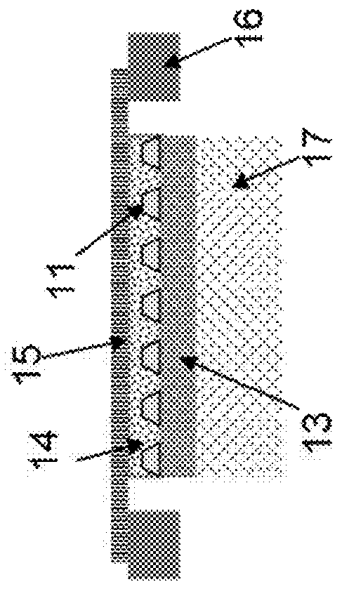
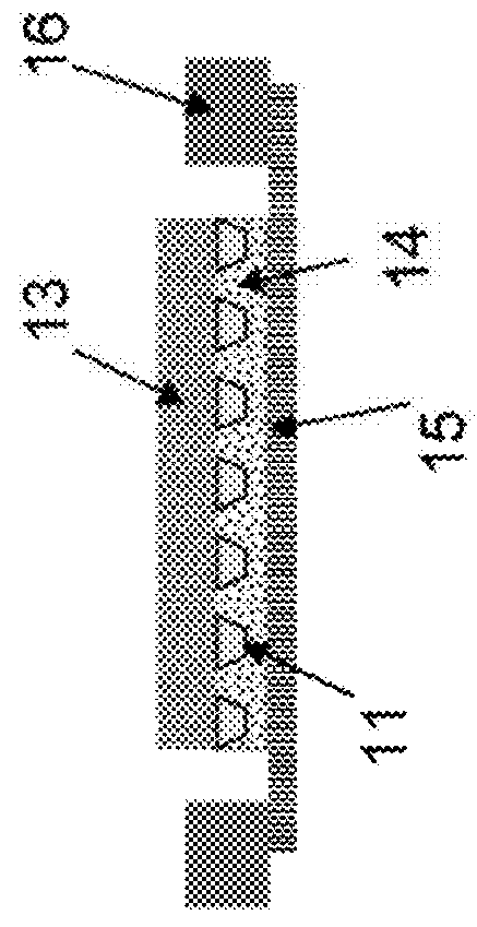
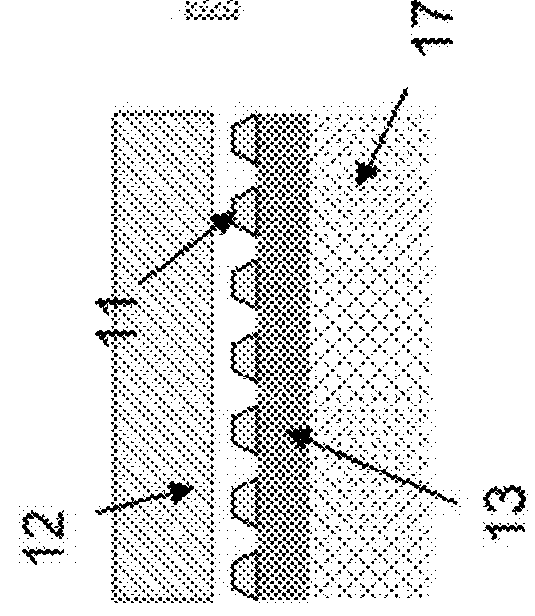
[0010]This invention is a method for the preparation of a semiconductor wafer for dicing. The semiconductor wafer has a plurality of metallic bumps on its active face. The essence of this invention is the use of a dicing tape having an underfill material disposed on one side. The dicing tape / underfill thus supplies the underfill material and the dicing tape in one step. Rather than applying an underfill material to the semiconductor wafer, and in a separate step, mounting the dicing tape over the underfill, the use of the combined dicing tape and underfill eliminates a step in the fabrication process. The assembly of dicing tape, underfill and wafer can be disposed in a dicing frame so that the inactive face of the wafer is oriented upwards, for ease in stealth dicing.

[0011]The wafer is prepared according to known methods from a semiconductor material, typically silicon, gallium arsenide, germanium, or similar compound semiconductor materials. The formation of the plurality of metal...


PUM


Abstract

A method for preparing a semiconductor with preapplied underfill comprises (a) providing a thinned silicon semiconductor wafer having a plurality of metallic bumps on its active face and, optionally, through-silica-vias vertically through the silicon semiconductor wafer; (b) providing an underfill material on a dicing support tape, in which the underfill material is precut to the shape of the semiconductor wafer; (c) aligning the underfill material on the dicing support tape with the semiconductor wafer and laminating the underfill material to the semiconductor wafer.

Description

BACKGROUND OF THE INVENTION[0001]This invention relates to a process for the fabrication of a semiconductor die.[0002]Miniaturization and slimming of electrical and electronic equipment has led to a need for both thinner semiconductor devices and thinner semiconductor packaging. One way to accomplish this is to thin down the wafer by removing excess material from the back side of the semiconductor wafer, typically done before the wafer is diced into individual semiconductor dies.[0003]Another solution to produce smaller and more efficient semiconductor packages is to utilize an array of metallic bumps attached to the active face of the wafer. The metallic bumps are disposed to match with bonding pads on a substrate. When the metal is reflowed to a melt, it connects with the bonding pads forming both electrical and mechanical connections. This metallic bump packaging is generally referred to as “flip chip” because the bumped semiconductors are flipped in order to be attached to their...

Claims


Application Information

Patent Timeline
Patent Type & Authority Patents(United States)
IPC IPC(8): H01L21/02H01L21/56H01L21/683H01L23/00
CPCH01L21/02002H01L21/561H01L21/563H01L21/6836H01L24/27H01L24/92H01L24/94H01L24/16H01L24/29H01L24/81H01L2221/6834H01L2221/68327H01L2221/68377H01L2224/16227H01L2224/27002H01L2224/27003H01L2224/27436H01L2224/2919H01L2224/29191H01L2224/73104H01L2224/81815H01L2224/9212H01L2224/94H01L2224/11H01L2224/27H01L2924/00014H01L2924/0665H01L2924/0635H01L2924/00012H01L21/304H01L2221/68368H01L21/78H01L2221/68381H01L2924/351H01L21/30H01L21/50
Inventor HOANG, GINAKIM, YOUNSANGGUINO, ROSE
Owner HENKEL KGAA
Learn More