Electrooptic device, method for driving electrooptic device and electronic apparatus

Active Publication Date: 2013-08-15
SEIKO EPSON CORP
View PDF4 Cites 26 Cited by
  • Summary
  • Abstract
  • Description
  • Claims
  • Application Information

AI Technical Summary

Benefits of technology

The invention aims to make electrooptic devices smaller and simpler without compromising display quality.

Problems solved by technology

In this case, display unevenness occurs and the display quality is degraded.

Method used


Image

  • Electrooptic device, method for driving electrooptic device and electronic apparatus
  • Electrooptic device, method for driving electrooptic device and electronic apparatus
  • Electrooptic device, method for driving electrooptic device and electronic apparatus

Examples


first embodiment

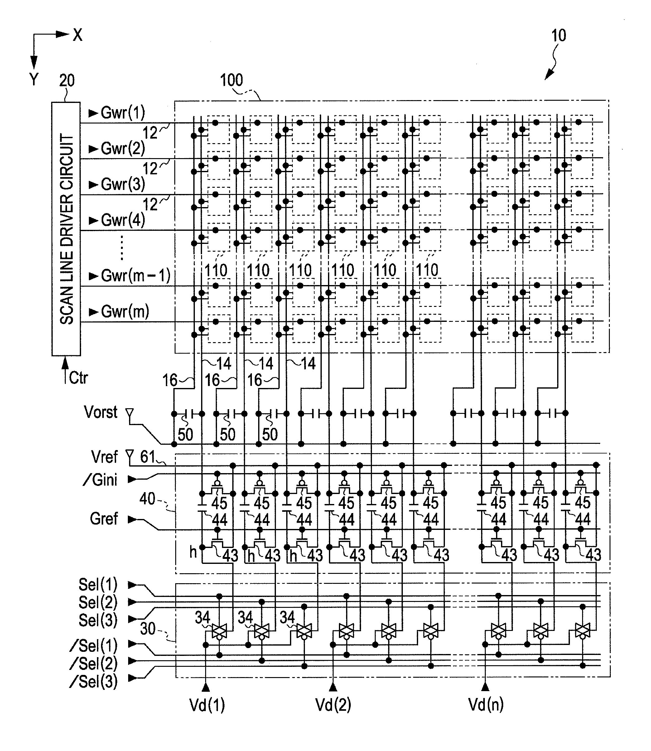
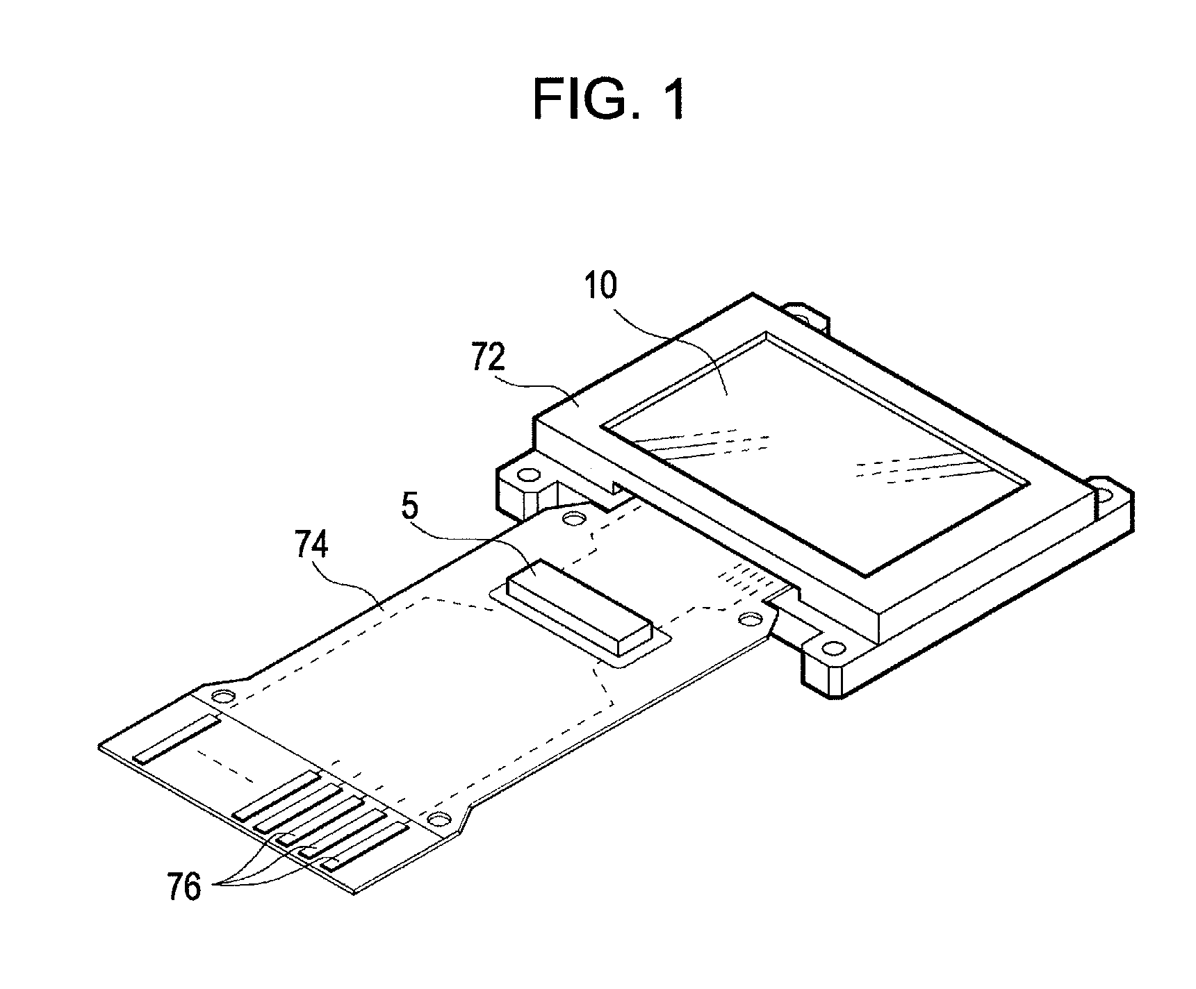
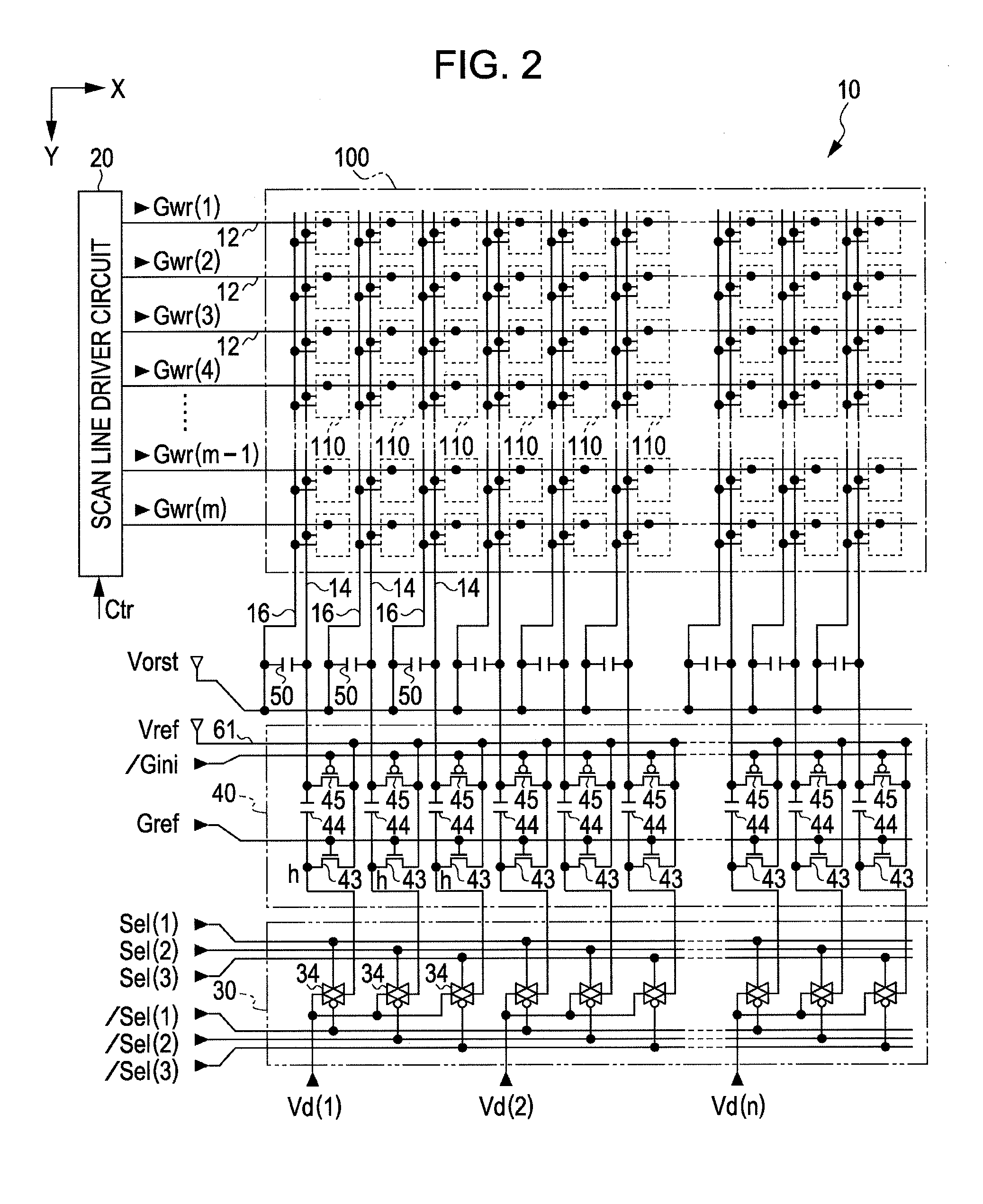
[0056]FIG. 1 is a perspective view which shows a structure of an electrooptic device 10 of an embodiment of the invention.

[0057]The electrooptic device 10 is a micro-display which displays an image, e.g., in a head mounted display. The electrooptic device 10 is an organic EL device in which a plurality of pixel circuits, driving circuits which drive the pixel circuits, etc., are formed, e.g., on a silicon substrate as described later in detail, and an exemplary light emitting element, an OLED, is used for the pixel circuit. The electrooptic device 10 is contained, e.g., in a frame-like case 72 which is open on a display section, and is connected with one end of an FPC (Flexible Printed Circuits) board 74. A control circuit 5 in a semiconductor chip is mounted on the FPC board 74 by means of COF (Chip On Film) technology, and the FPC board 74 is provided with a plurality of terminals 76 and is connected with an upper rank circuit which is omitted to be shown. The upper rank circuit p...

second embodiment

[0148]The first embodiment is structured in such a way that the other end of the holding capacitor 44 of each of the columns, i.e., the node h is directly provided with a data signal by the demultiplexer 30. Thus, as the period of time in which a data signal is provided by the control circuit 5 equals the period for writing in the period for scanning each of the rows, temporal limitation is significant.

[0149]Thus, a second embodiment which can alleviate such temporal limitation will be explained next. Incidentally, portions different from corresponding ones of the first embodiment will be mainly explained below in order that a repeated explanation is avoided.

[0150]FIG. 11 illustrates a structure of an electrooptic device 10 of a second embodiment.

[0151]The second embodiment shown in the drawing is different from the first embodiment shown in FIG. 2 mainly in that the columns in the level shift circuit 40 are each provided with a holding capacitor 41 (fourth holding capacitor) and a ...


PUM


Abstract

An electrooptic device has a data line, a pixel circuit and a driver circuit which drives the pixel circuit. The driver circuit has a first feeder line, a level shift circuit to be electrically coupled with the data line and a driving control circuit which provides the first feeder line with a first voltage or a second voltage and controls operations of the level shift circuit and the pixel circuit. The level shift circuit has a second holding capacitor and a switch section which switches over condition of a connection between the second holding capacitor and the first feeder line.

Description

BACKGROUND[0001]1. Technical Field[0002]The present invention relates to an electrooptic device, a method for driving an electrooptic device and an electronic apparatus.[0003]2. Related Art[0004]Various kinds of electrooptic devices using light emitting elements including an organic light emitting diode (OLED) are proposed in recent years. Such an electrooptic device is generally structured to be provided with a pixel circuit including the light emitting element described above, a transistor, etc., correspondingly to a crossing of a scan line and a data line correspondingly to a pixel of an image to be displayed, e.g., as disclosed in JP-A-2007-316462.[0005]Incidentally, a demand for application of an electrooptic device using a light emitting element to a small-sized apparatus such as a portable apparatus, a head mounted display, etc., grows in recent years. In this case, it is necessary to downsize the electrooptic device without degrading a display quality. Further, it is desirab...

Claims


Application Information

Patent Timeline
IPC IPC(8): H05B37/02
CPCG09G2320/045G09G3/3241H05B37/02G09G3/3291G09G2300/0819G09G2300/0861G09G2300/0814G09G2320/0233H05B47/10
Inventor OTA, HITOSHIFUJITA, SHIN
Owner SEIKO EPSON CORP
Why Eureka
Try Eureka