Non-planar mosfet structures with asymmetric recessed source drains and methods for making the same

a mosfet and source drain technology, applied in the field of metal oxide semiconductor field effect transistors, can solve the problems of reducing device performance, high resistance on the source side, and reducing the performance of fets, so as to reduce external resistance and reduce fringing capacitance

Active Publication Date: 2013-08-22
GLOBALFOUNDRIES US INC
View PDF2 Cites 65 Cited by
  • Summary
  • Abstract
  • Description
  • Claims
  • Application Information

AI Technical Summary

Benefits of technology

[0010]An advantage of the present invention is reduced fringing capacitance and reduced external resistance.
[0011]A further advantage of the present, is the ability to make a chip having numerous device configurations including: source up with asymmetric source/drains, source down with asymmetric source/drains, and symmetric source/drains.
[0012]Another advantage of the present invention is the ability to create symmetric and asymmetric channels within the same tri-gate device.
[0013]Other characteristics and

Problems solved by technology

Extrinsic resistance (herein “Rext”) and fringing capacitances reduce the performance of FETs, including finFET and tri-gate transistors.
In particular high capacitance in the drain side of a transistor and high resistance on the source side reduce device performance.
However, techniques associated with reduc

Method used


Image

  • Non-planar mosfet structures with asymmetric recessed source drains and methods for making the same
  • Non-planar mosfet structures with asymmetric recessed source drains and methods for making the same
  • Non-planar mosfet structures with asymmetric recessed source drains and methods for making the same

Examples


Embodiment Construction

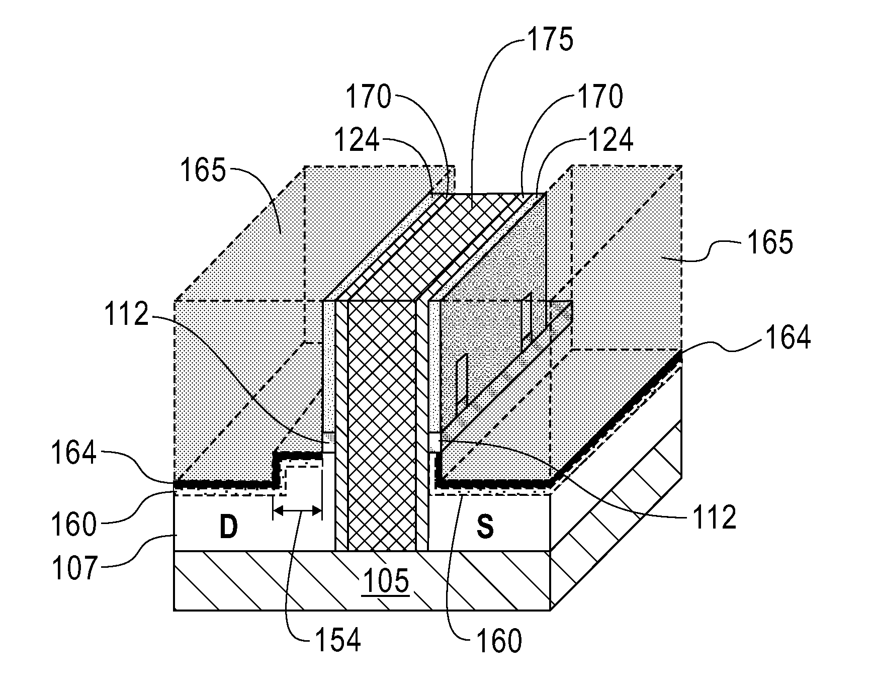
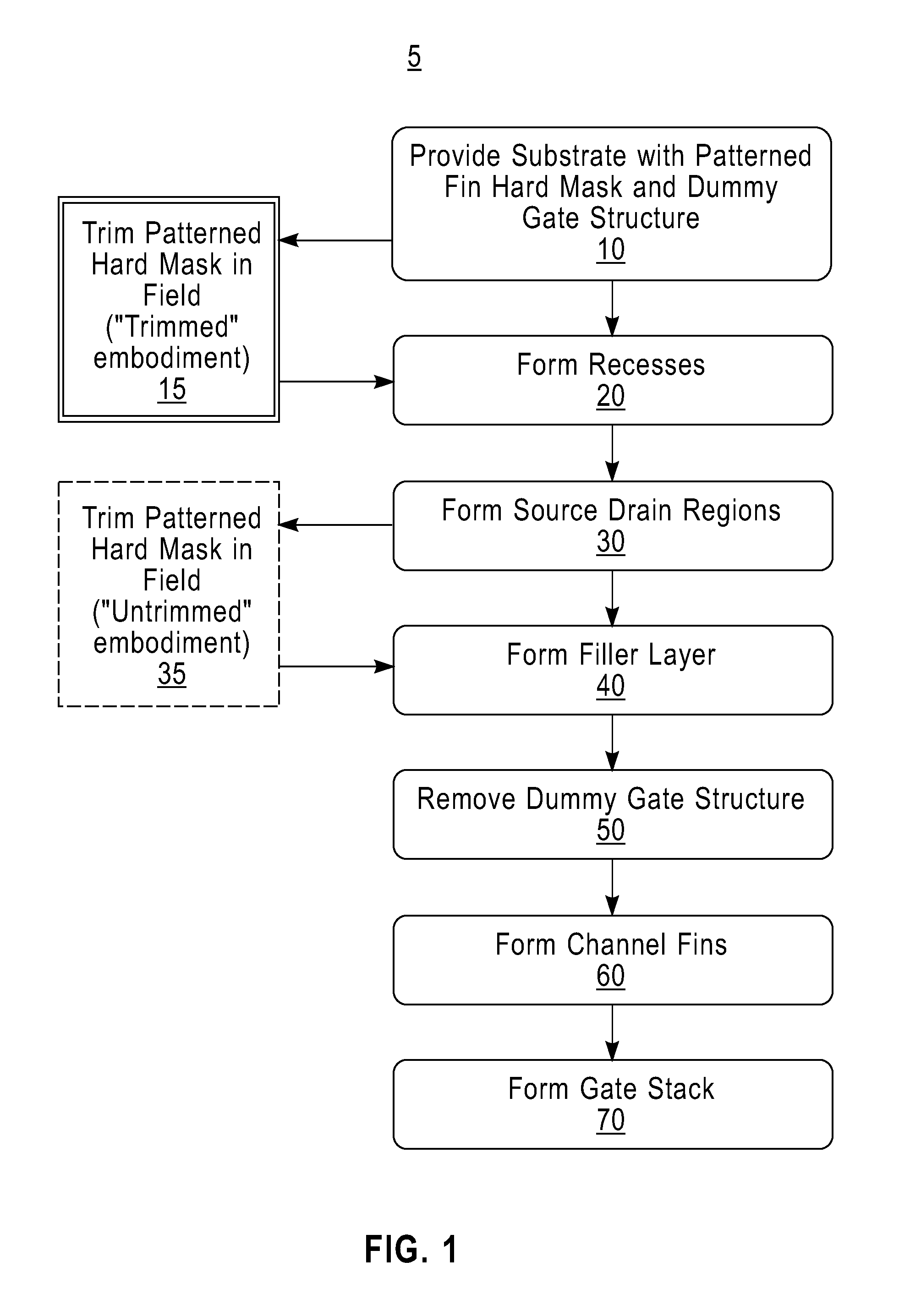
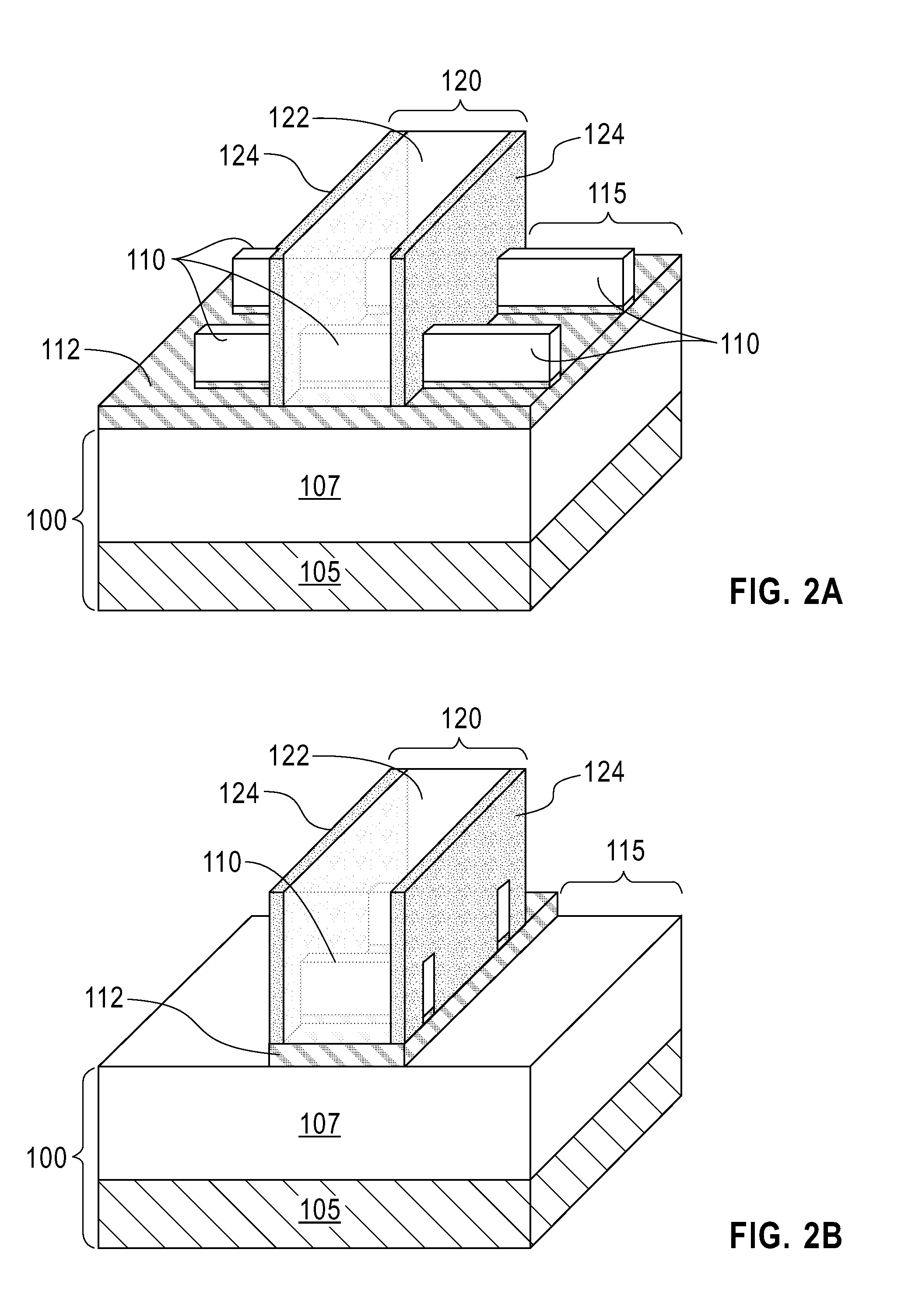
[0053]The basic principle of the invention is a method of making non-planar MOSFETs having reduced source-side Rext and drain-side fringing capacitance. The method includes untrimmed and trimmed embodiments which will be described in conjunction with FIGS. 1-13. The method also includes a method of making a plurality of non-planar transistor having different configurations including asymmetric source up, asymmetric source down and symmetric. The invention further includes structures of non-planar transistors made by the untrimmed and trimmed methods. The structures will be described in conjunction with FIGS. 14 and 15. A detailed description of the invention is made in combination with the following embodiments.

Methods

[0054]FIG. 1 is a flow chart 5 with the steps of creating a non-planar MOSFET with asymmetric, recessed source drains according to untrimmed and trimmed embodiments. In both embodiments a fin-last, replacement gate process is used to create the device. Steps common to ...


PUM


Abstract

Non-planar Metal Oxide Field Effect Transistors (MOSFETs) and methods for making non-planar MOSFETs with asymmetric, recessed source and drains having improved extrinsic resistance and fringing capacitance. The methods include a fin-last, replacement gate process to form the non-planar MOSFETs and employ a retrograde metal lift-off process to form the asymmetric source/drain recesses. The lift-off process creates one recess which is off-set from a gate structure while a second recess is aligned with the structure. Thus, source/drain asymmetry is achieved by the physical structure of the source/drains, and not merely by ion implantation. The resulting non-planar device has a first channel of a fin contacting a substantially undoped area on the drain side and a doped area on the source side, thus the first channel is asymmetric. A channel on atop surface of a fin is symmetric because it contacts doped areas on both the drain and source sides.

Description

BACKGROUND OF THE INVENTION[0001]1. Field of the Invention[0002]The present invention generally relates to a Metal Oxide Semiconductor Field Effect Transistors (MOSFETs). In particular, the invention relates to non-planar MOSFETs (i.e. FinFET or tri-gate transistors) with asymmetric recessed source and drains having reduced source-side extrinsic resistance and drain-side fringing capacitance and methods of making the same. The methods include using a fin-last, replacement gate process to form the non-planar MOSFETs and, in particular, employ a retrograde metal lift-off process to form the asymmetric source / drain recesses.[0003]2. Description of Related Art[0004]Extrinsic resistance (herein “Rext”) and fringing capacitances reduce the performance of FETs, including finFET and tri-gate transistors. In particular high capacitance in the drain side of a transistor and high resistance on the source side reduce device performance. Methods of fabricating and structures that reduce resistan...

Claims


Application Information

Patent Timeline
IPC IPC(8): H01L29/786H01L21/336
CPCH01L29/66545H01L29/0657H01L29/66795
Inventor CHANG, JOSEPHINE B.CHANG, PAULGUILLORN, MICHAEL A.LIN, CHUNG-HSUNSLEIGHT, JEFFREY W.
Owner GLOBALFOUNDRIES US INC
Why Eureka
Try Eureka