Embedded touch screen

a touch screen and touch technology, applied in the field of embedded touch screens, can solve the problems of increasing the number of manufacturing steps, the thickness and weight of the touch panel, and the cost of the components, so as to achieve the effect of low noise and high detection sensitivity

Active Publication Date: 2013-08-22
PANASONIC INTELLECTUAL PROPERTY CORP OF AMERICA
View PDF10 Cites 20 Cited by
  • Summary
  • Abstract
  • Description
  • Claims
  • Application Information

AI Technical Summary

Benefits of technology

[0046]According to the aspect of Item (17) or (18) of the present invention, it is possible to obtain the embedded touch screen which is less affected by noise and has high detection sensitivity.
[0047]According to the aspect of Item (19) of the present invention, the coordinate detection can be performed without affecting an image to be displayed.
[0048]According to the aspect of Item (20) of the present invention, the coordinate detection can be performed without decreasing brightness of an image to be displayed.

Problems solved by technology

Such a touch panel has disadvantages in panel thickness and weight, the number of components, and its cost.
Further, the number of manufacturing steps increases, and hence there arises a problem of decreasing yields.
Particularly in a small-sized or high resolution image display device, the TFT originally occupies a large area in proportion to the entire pixel, and hence it is not very realistic to further increase the number of TFTs in the pixel.
In the embedded touch screen described in JP 2011-527787 A, the common electrode needs to be divided into complicated shapes, and the contact detection is performed for each block, which degrades the accuracy of coordinate detection.

Method used


Image

  • Embedded touch screen
  • Embedded touch screen
  • Embedded touch screen

Examples


embodiment 1

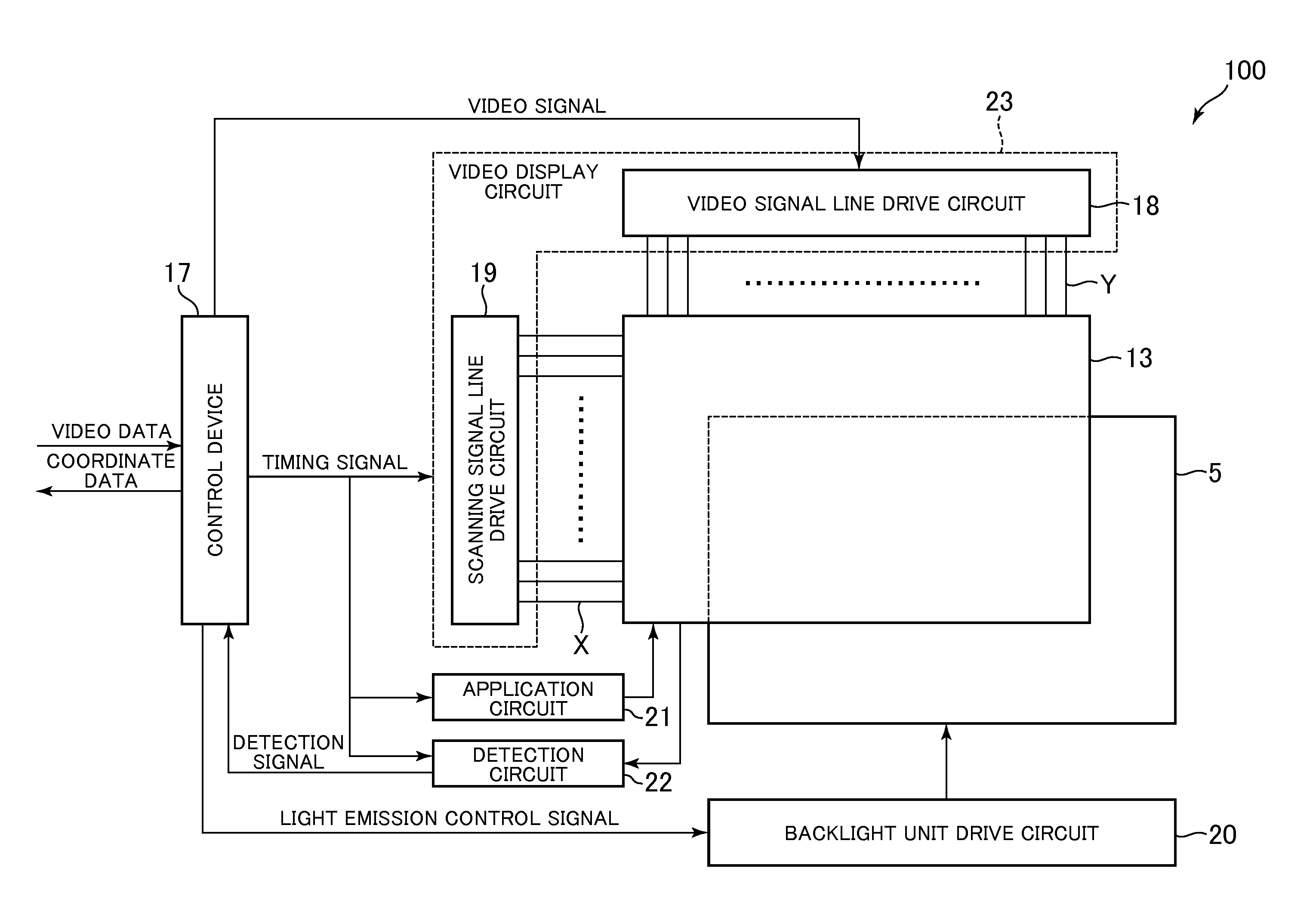
[0079]FIG. 3 is a view illustrating a configuration of an embedded touch screen 100 according to Embodiment 1 of the present invention.

[0080]A liquid crystal panel 13 has a rectangular shape, and has lateral and vertical lengths determined depending on the application of the embedded touch screen 100. The liquid crystal panel 13 illustrated in FIG. 3 has a laterally long shape (the lateral length is larger than the vertical length). However, the shape of the liquid crystal panel 13 is not limited thereto, and the liquid crystal panel 13 may have a vertically long shape (the lateral length is smaller than the vertical length), or the lateral length may be the same as the vertical length.

[0081]On the second substrate 3 of the liquid crystal panel 13, a plurality of video signal lines Y and a plurality of scanning signal lines X are formed. The video signal line Y and the scanning signal line X are provided orthogonal to each other, and are formed into a lattice shape. A region surroun...

embodiment 2

[0118]FIG. 11 is a view schematically illustrating an overall configuration of an embedded touch screen 200 according to Embodiment 2 of the present invention for contact detection and coordinate detection. Note that, detailed structures of the embedded touch screen 200 other than those illustrated in FIG. 11 are similar to those in the embedded touch screen 100 according to Embodiment 1 described above, and hence redundant description thereof is omitted.

[0119]The embedded touch screen 200 uses the video signal shielding electrodes 26 as the detection electrode RC, and uses the pixel electrodes 15 as the excitation electrode EX. Therefore, the application circuit 21 is connected to the video signal lines 25 connected to the respective pixel electrodes 15, and the detection circuit 22 is connected to the video signal shielding electrodes 26. Further, the scanning circuit 35 scans the pixel electrodes 15 for each of the scanning units, and hence in this embodiment, the excitation elec...

embodiment 3

[0121]FIG. 12 is a view schematically illustrating an overall configuration of an embedded touch screen 300 according to Embodiment 3 of the present invention for contact detection and coordinate detection. Note that, detailed structures of the embedded touch screen 300 other than those illustrated in FIG. 12 are also similar to those in the embedded touch screen 100 according to Embodiment 1 described above, and hence redundant description thereof is omitted.

[0122]In the embedded touch screen 300, the pixel electrodes 15 are used as both the excitation electrode EX and the detection electrode RC. Therefore, the application circuit 21 is connected to the video signal lines 25 connected to the pixel electrodes 15 to be used as the excitation electrode EX, and the detection circuit 22 is connected to the video signal lines 25 connected to the pixel electrode 15 to be used as the detection electrode RC. Further, the scanning circuit 35 scans the pixel electrodes 15 for each of the scan...


PUM


Abstract

Provided is an embedded touch screen, including: a first substrate; a second substrate including: scanning signal lines extending in a first direction; video signal lines extending in a second direction; a plurality of pixels each including a pixel electrode connected to corresponding one of the video signal lines via a switching element connected to corresponding one of the scanning signal lines; and a common electrode; a liquid crystal layer; an application circuit for applying an alternating signal to a plurality of excitation electrodes; a detection circuit for detecting a signal excited on a plurality of detection electrodes each arranged adjacent to each of the plurality of excitation electrodes; and a scanning circuit for scanning at least one of each of the plurality of excitation electrodes and each of the plurality of detection electrodes at least in the second direction.

Description

CROSS-REFERENCE TO RELATED APPLICATION[0001]The present application claims priority from Japanese application JP 2012-033837 filed on Feb. 20, 2012, the content of which is hereby incorporated by reference into this application.BACKGROUND OF THE INVENTION[0002]1. Field of the Invention[0003]The present invention relates to an embedded touch screen.[0004]2. Description of the Related Art[0005]A tablet-type information terminal and a multifunctional mobile phone (so-called smartphone) including a touch screen have become popular. The “touch screen” as used herein refers to a device obtained by combining a touch panel to an image display device such as a liquid crystal display device. Further, the “touch panel” as used herein refers to a planar contact-detection type pointing device. A user directly touches the touch screen with a finger, a stylus, or the like while looking at an image displayed on the screen, thereby performing input.[0006]The generally popularized touch screen is obt...

Claims


Application Information

Patent Timeline
Patent Type & Authority Applications(United States)
IPC IPC(8): G09G3/36
CPCG06F3/044G09G3/3611G06F3/0445
Inventor KAWACHI, GENSHIROKITA, KAZUOONO, KIKUO
Owner PANASONIC INTELLECTUAL PROPERTY CORP OF AMERICA
Why Eureka
Try Eureka