Semiconductor device and method for manufacturing the same

a semiconductor and semiconductor technology, applied in the direction of semiconductor devices, electrical appliances, transistors, etc., can solve the problems that contact resistance significantly affects the on-state current characteristics, and achieve the effect of reducing contact resistance, reducing resistance of sources or drains of transistors, and reducing resistan

Active Publication Date: 2013-08-29
SEMICON ENERGY LAB CO LTD
View PDF8 Cites 34 Cited by
  • Summary
  • Abstract
  • Description
  • Claims
  • Application Information

AI Technical Summary

Benefits of technology

[0010]In view of the above, an object of one embodiment of the present invention is to provide a semiconductor device in which a decrease in the on-state current is suppressed by lowering the parasitic resistance value.
[0018]Further, an oxygen vacancy in an oxide semiconductor is a cause of generation of a carrier. Thus, the impurity region has lower resistance than the channel formation region and serves as a source region or a drain region of a transistor. With the impurity region, resistance of a source or a drain of the transistor can be reduced. In addition, when the source electrode layer or the drain electrode layer is in contact with the oxide semiconductor layer at the impurity region, the contact resistance can be reduced.
[0019]Since an oxygen vacancy in the oxide semiconductor causes generation of carrier, a large number of oxygen vacancies in the channel formation region of a transistor leads to generation of electrons serving as a carrier in the channel formation region and is thus a factor causing the shift of the threshold voltage of the transistor in the negative direction. Thus, in order to improve the reliability of the transistor, it is important for providing an impurity region that generation of oxygen vacancies in the channel formation region be reduced as much as possible.
[0020]In the transistor according to one embodiment of the present invention, the vicinity of the channel formation region (more specifically, a region overlapping with the sidewall insulating layer) in the oxide semiconductor layer contains no impurity element or contains an impurity element at a lower concentration than regions in the oxide semiconductor layer, which are in contact with the source electrode layer and the drain electrode layer. Thus, introduction of impurity into the channel formation region can be effectively suppressed.

Problems solved by technology

However, when the channel length L is decreased, the parasitic resistance that is the sum of the resistance between a source and a channel, the resistance between a drain and the channel and the contact resistance significantly affects the on-state current characteristics.

Method used


Image

  • Semiconductor device and method for manufacturing the same
  • Semiconductor device and method for manufacturing the same
  • Semiconductor device and method for manufacturing the same

Examples


embodiment 1

[0040]In this embodiment, one embodiment of a semiconductor device and a method for manufacturing the semiconductor device will be described with reference to FIGS. 1A to 1C, FIGS. 2A to 2C, and FIGS. 3A to 3C. In this embodiment, a transistor including an oxide semiconductor layer is shown as an example of the semiconductor device.

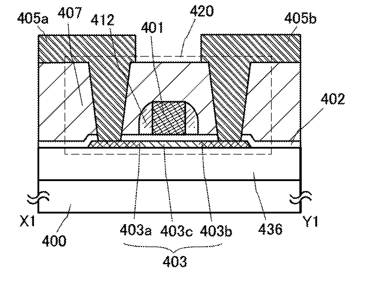
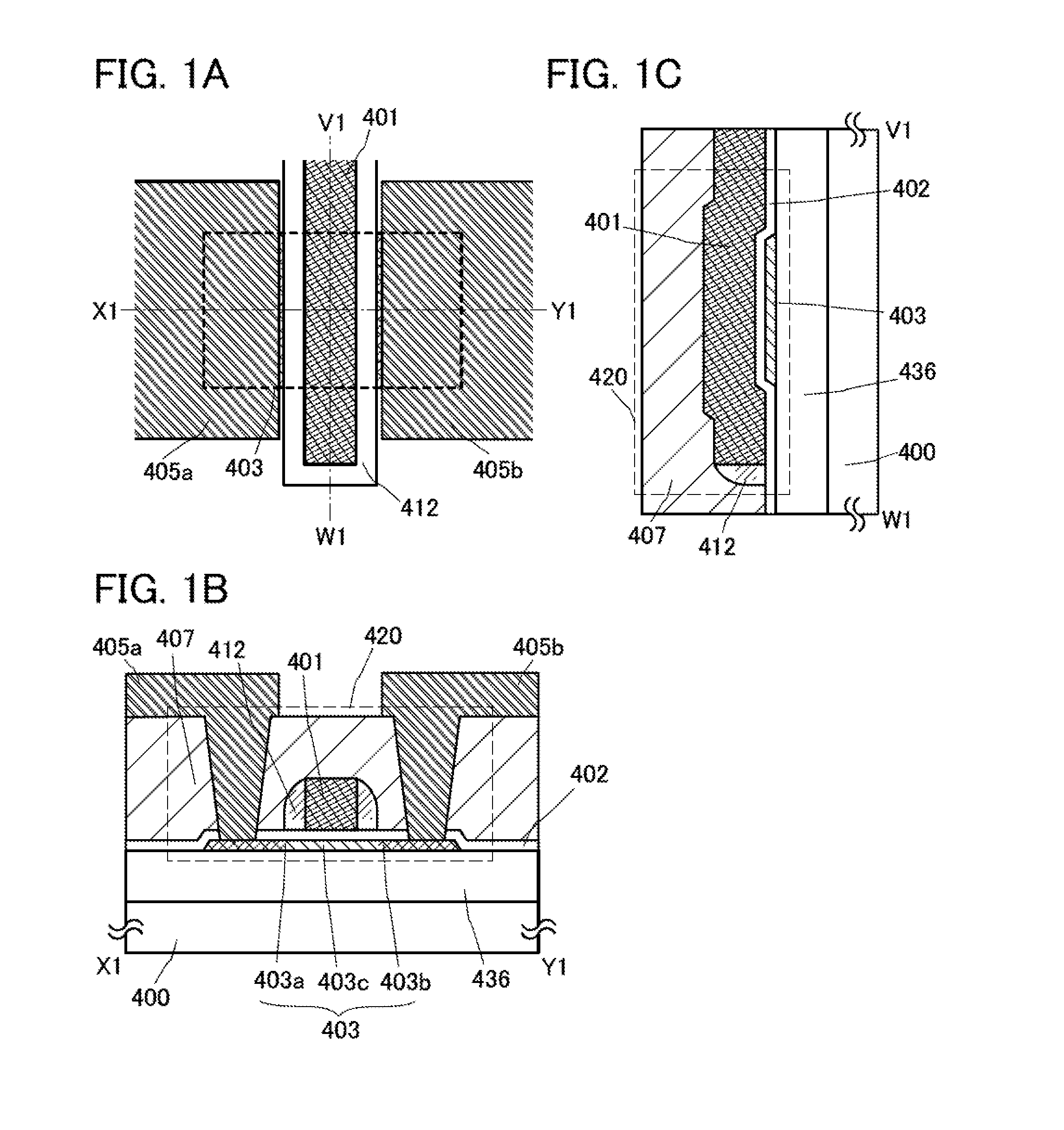
[0041]FIGS. 1A to 1C illustrate a structure example of a transistor 420. FIG. 1A is a plan view of the transistor 420, FIG. 1B is a cross-sectional view taken along the line X1-Y1 in FIG. 1A, and FIG. 1C is a cross-sectional view taken along the line V1-W1 in FIG. 1A. Note that in FIG. 1A, some components of the transistor 420 (e.g., an insulating layer 407 and the like) are not illustrated to avoid complexity.

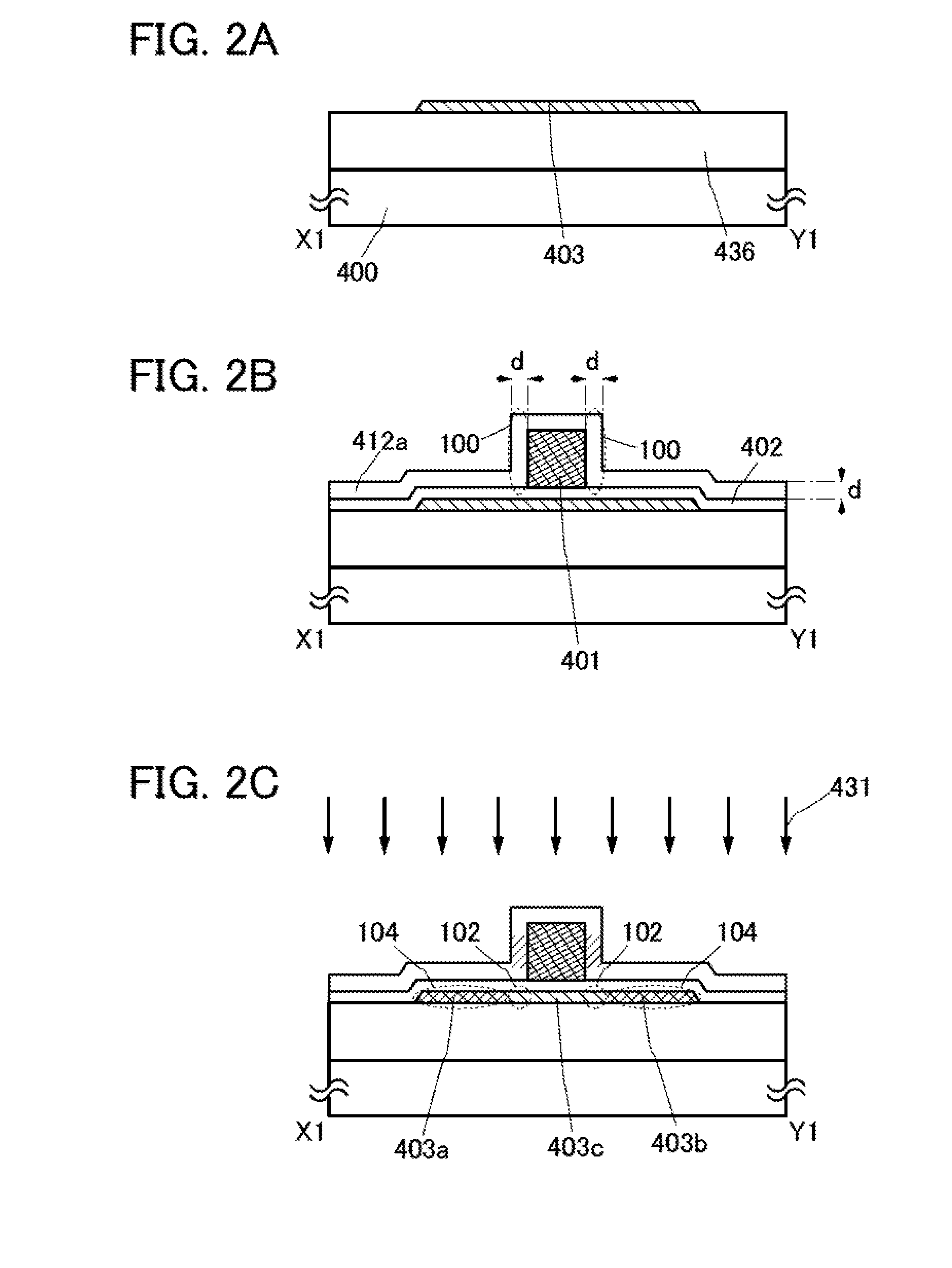
[0042]The transistor 420 illustrated in FIGS. 1A to 1C includes the following components over a substrate 400: an oxide semiconductor layer 403 which includes a pair of impurity regions 403a and 403b and a channel formation region 403c; a gate insul...

embodiment 2

[0142]In this embodiment, a semiconductor device with a different structure from that of Embodiment 1 and a method for manufacturing the semiconductor device will be described with reference to FIGS. 4A to 4C and FIGS. 5A to 5D. The same portions as those in the above embodiment, portions having functions similar to those of the portions in the above embodiment, and steps similar to those in the above embodiment may be carried out as in the above embodiment, and repeated description is omitted. In addition, detailed description of the same portion is not repeated.

[0143]FIGS. 4A to 4C illustrate a structure example of a transistor 422. FIG. 4A is a plan view of the transistor 422, FIG. 4B is a cross-sectional view taken along line X2-Y2 in FIG. 4A, and FIG. 4C is a cross-sectional view taken along line V2-W2 in FIG. 4A. Note that in FIG. 4A, some components of the transistor 422 (e.g., an insulating layer 414 and the like) are not illustrated to avoid complexity.

[0144]The transistor ...

embodiment 3

[0161]In this embodiment, an example of a semiconductor device (memory device) which includes the transistor described in this specification, which can hold stored data even when not powered, and which has an unlimited number of write cycles will be described with reference to drawings.

[0162]FIGS. 6A and 6B illustrate one example of a structure of the semiconductor device. FIG. 6A is a cross-sectional view of the semiconductor device, FIG. 6B is a plan view of the semiconductor device, and FIG. 6C is a circuit diagram of the semiconductor device. Here, FIG. 6A corresponds to cross sections taken along line C1-C2 and line D1-D2 in FIG. 6B.

[0163]The semiconductor device illustrated in FIGS. 6A and 6B includes a transistor 160 including a first semiconductor material in a lower portion, and a transistor 162 including a second semiconductor material in an upper portion. For the transistor 162, the structure of the transistor 422 shown in Embodiment 2 is employed as an example.

[0164]Here...


PUM


Abstract

An oxide semiconductor layer is formed, a gate insulating layer is formed over the oxide semiconductor layer, a gate electrode layer is formed to overlap with the oxide semiconductor layer with the gate insulating layer interposed therebetween, a first insulating layer is formed to cover the gate insulating layer and the gate electrode layer, an impurity element is introduced through the insulating layer to form a pair of impurity regions in the oxide semiconductor layer, a second insulating layer is formed over the first insulating layer, the first insulating layer and the second insulating layer are anisotropically etched to form a sidewall insulating layer in contact with a side surface of the gate electrode layer, and a source electrode layer and a drain electrode layer in contact with the pair of impurity regions are formed.

Description

BACKGROUND OF THE INVENTION[0001]1. Field of the Invention[0002]The disclosed invention relates to a semiconductor device and a method for manufacturing the semiconductor device.[0003]In this specification and the like, a semiconductor device refers to all types of devices which can function by utilizing semiconductor characteristics; an electro-optical device, a light-emitting display device, a semiconductor circuit, and an electronic device are all semiconductor devices.[0004]2. Description of the Related Art[0005]A technique by which transistors are formed using semiconductor thin films formed over a substrate having an insulating surface has been attracting attention. The transistor is applied to a wide range of semiconductor devices such as an integrated circuit (IC) and an image display device (also simply referred to as display device). A silicon-based semiconductor material is widely known as a material for a semiconductor thin film applicable to a transistor. As another mat...

Claims


Application Information

Patent Timeline
Patent Type & Authority Applications(United States)
IPC IPC(8): H01L29/786H01L29/66
CPCH01L29/66742H01L29/7869H01L21/02565H01L21/02595H01L21/02631H01L29/04H01L29/24H01L29/66969H01L29/78603
Inventor ISOBE, ATSUOTEZUKA, SACHIAKIOHNO, SHINJI
Owner SEMICON ENERGY LAB CO LTD
Why Eureka
Try Eureka