Semiconductor device and manufacturing method thereof

a technology of semiconductors and semiconductors, applied in the direction of light-sensitive devices, electrolytic capacitors, coatings, etc., can solve the problems of increasing unstable fabrication process, and reducing the on-state current, so as to reduce the on-state current, reduce the number of steps, and improve the effect of manufacturing method

Inactive Publication Date: 2008-09-11
SEMICON ENERGY LAB CO LTD
View PDF24 Cites 8 Cited by
  • Summary
  • Abstract
  • Description
  • Claims
  • Application Information

AI Technical Summary

Benefits of technology

[0012]In a semiconductor device of the present invention, the thickness of a source region or a drain region is arranged to be larger than the thickness of a channel formation region. This feature is achieved by melting the semiconductor layer formed over an insulating layer provided with a projection portion and a depression portion to planalize the surface of the semiconductor layer. Therefore, the semiconductor device in which subthreshold swing is low and a decrease in the on-state current is suppressed can be manufactured. In addition, since the surface of the semiconductor layer is planarized by melting the semiconductor layer, a semiconductor device can be easily manufactured without increasing the number of processes.
[0013]Accordingly, in the present invention, a semiconductor device in which subthreshold swing is low and a decrease in the on-state current is suppressed and which has a good response can be easily manufactured.

Problems solved by technology

However, there have been problems such that the resistance of each of a source region and a drain region and the contact resistance are increased by reducing the thickness of the semiconductor layer, which leads to a decrease in the on-state current.
However, as described in Patent Document 1, there is a problem in that the fabrication process is unstable because the formation of a semiconductor layer having different thicknesses on a flat surface of an insulating substrate requires selective etching of the semiconductor layer to form a channel formation region with a desired thickness.
In the method described in Patent Document 2, there is a problem in that the number of steps is increased because etching treatment is performed in order to planarize the surface of a semiconductor layer and a process is unstable because selective etching treatment of the semiconductor layer is required to form the semiconductor layer with a planarized surface.
In addition, there is a problem in that a process is unstable because well-controlled etching treatment of the Si film is required.
Particularly, it is quite difficult to control the thickness of the semiconductor layer in an attempt to fabricate the channel formation region with a thickness of 50 nm or less.

Method used


Image

  • Semiconductor device and manufacturing method thereof
  • Semiconductor device and manufacturing method thereof
  • Semiconductor device and manufacturing method thereof

Examples


embodiment mode 1

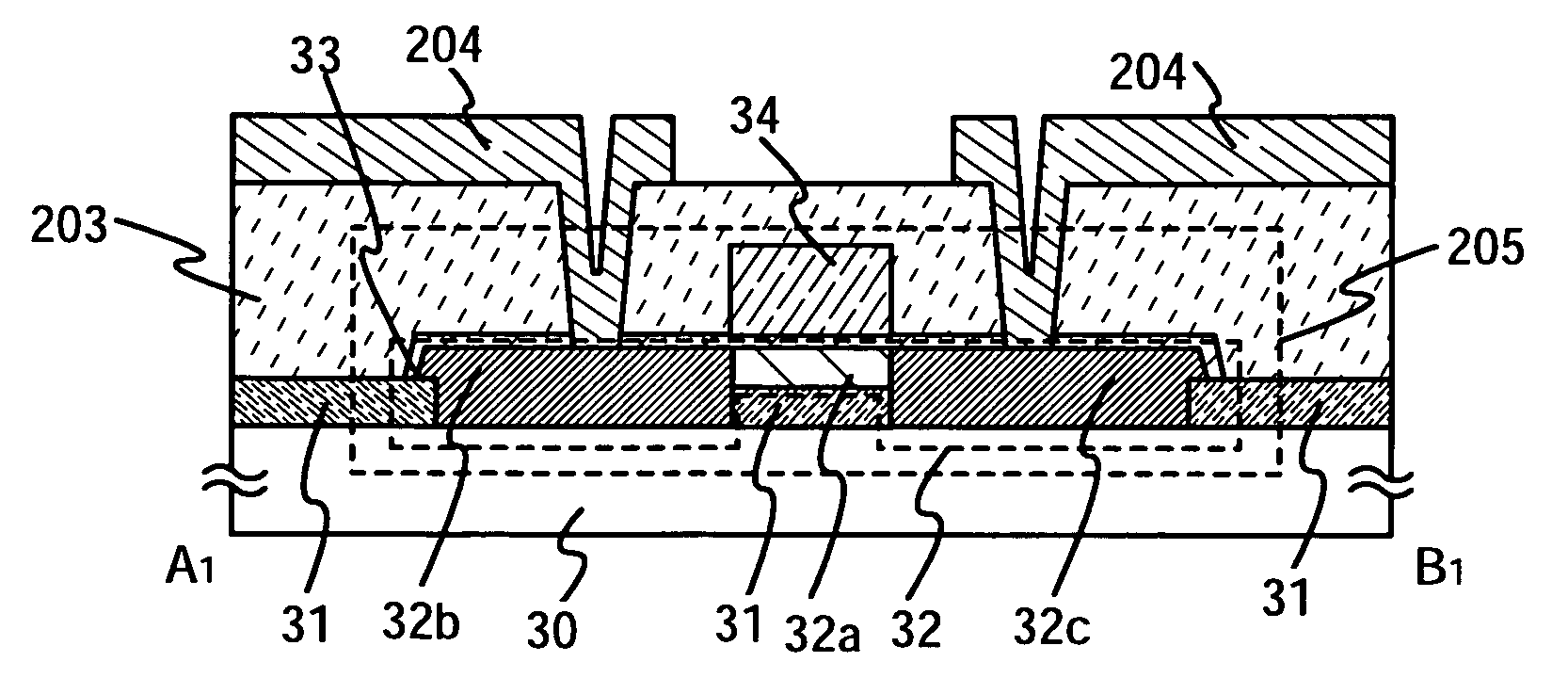
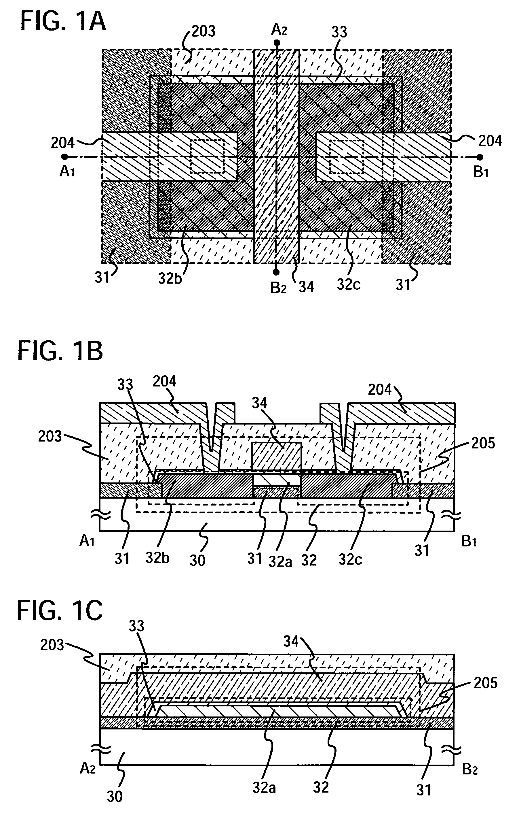
[0031]In this embodiment mode, a structure of a semiconductor device formed using a semiconductor layer in which the thickness of a source region or a drain region is larger than the thickness of a channel formation region and a manufacturing method thereof will be described.

[0032]FIG. 1A is a top view and FIGS. 1B and 1C are cross-sectional views used to describe a structure of a semiconductor device of the present invention. FIG. 1A is a top view of a semiconductor device formed using a thin film transistor. FIG. 1B is a cross-sectional view taken along a dashed line connecting a point A1 and a point B1 of FIG. 1A. FIG. 1C is a cross-sectional view taken along a dashed line connecting a point A2 and a point B2 of FIG. 1A.

[0033]The semiconductor device given in this embodiment mode includes a thin film transistor 205 having an insulating layer 31 which is provided such that a projection portion and a depression portion are formed over a substrate 30, an island-shaped semiconductor ...

embodiment mode 2

[0067]In this embodiment mode, a method for manufacturing a semiconductor device of the present invention which includes a thin film transistor, a memory element, and an antenna will be described with reference to the drawings.

[0068]FIGS. 7A and 7B show a top view and a cross-sectional view, respectively, each illustrating a structure of a semiconductor device given in this embodiment mode. Note that an example of an upper surface structure of a semiconductor device given in this embodiment mode is shown in FIG. 7A, and a part of a cross-sectional structure of FIG. 7A is shown in FIG. 7B.

[0069]In this embodiment mode, a semiconductor device 200 includes an integrated circuit portion 201, a memory portion 202, and an antenna 303 (FIG. 7A). Note that, in FIG. 7B, a region 304 corresponds to a part of a cross-sectional structure of the integrated circuit portion 201 of FIG. 7A, a region 305 corresponds to a part of a cross-sectional structure of the memory portion 202 of FIG. 7A, and a...

embodiment mode 3

[0105]In this embodiment mode, an example of a block diagram of a semiconductor device which is capable of inputting and outputting data without contact will be described. According to its usage mode, a semiconductor device capable of inputting and outputting data without contact may also be referred to as an RFID tag, an ID tag, an IC tag, an IC chip, an RF tag, a wireless tag, an electronic tag, or a wireless chip.

[0106]FIG. 12 shows a block diagram for describing a structure of a semiconductor device which is capable of inputting and outputting data without contact. A semiconductor device 800 which is capable of inputting and outputting data without contact has a function of communicating data with a reader / writer without contact and includes a high-frequency circuit 810, a power supply circuit 820, a reset circuit 830, a clock generation circuit 840, a data demodulation circuit 850, a data modulation circuit 860, a control circuit 870 which controls another circuit, a memory cir...


PUM

PropertyMeasurementUnit
thicknessaaaaaaaaaa
thicknessaaaaaaaaaa
angleaaaaaaaaaa

Abstract

A semiconductor device having a highly responsive thin film transistor (TFT) with low subthreshold swing and suppressed decrease in the on-state current and a manufacturing method thereof are demonstrated. The THF of the present invention is characterized by its semiconductor layer where the thickness of the source region or the drain region is larger than that of the channel formation region. Manufacture of the TFT is readily achieved by the formation of an amorphous semiconductor layer on a projection portion and a depression portion, which is followed by subjecting the melting process of the semiconductor layer, resulting in the formation of a crystalline semiconductor layer having different thicknesses. Selective addition of impurity to the thick portion of the semiconductor layer provides a semiconductor layer in which the channel formation region is thinner than the source or drain region.

Description

BACKGROUND OF THE INVENTION[0001]1. Field of the Invention[0002]The present invention relates to a semiconductor device and a manufacturing method thereof.[0003]2. Description of the Related Art[0004]In recent years, manufacturing of semiconductor devices in which thin film transistors (hereinafter referred to as TFTs) formed over insulating surfaces of substrates such as glass are utilized as switching elements or the like has been actively pursued. For these thin film transistors, a structure is proposed in which island-shaped semiconductor layers are formed over a substrate having an insulating surface by a CVD method, a photolithography method, or the like, and a part of the island-shaped semiconductor layers is utilized as a channel formation region.[0005]In such a situation, in order to improve characteristics of a thin film transistor, a method for forming a thin film transistor is proposed in which subthreshold swing (here, the subthreshold swing (S value) is referred to as ...

Claims


Application Information

Patent Timeline
Patent Type & Authority Applications(United States)
IPC IPC(8): H01L21/84
CPCH01L21/0237H01L21/02675H01L27/1281H01L29/78696H01L21/02691
Inventor OHNUMA, HIDETOISOBE, ATSUOGODO, HIROMICHI
Owner SEMICON ENERGY LAB CO LTD
Why Eureka
Try Eureka