Lead frame for mounting LED elements, lead frame with resin, method for manufacturing semiconductor devices, and lead frame for mounting semiconductor elements
- Summary
- Abstract
- Description
- Claims
- Application Information
AI Technical Summary
Benefits of technology
Problems solved by technology
Method used
Image

Examples
first embodiment
[0092]Hereunder, a first embodiment of the present invention will be described referring to the accompanying drawings. FIGS. 1 to 6 show the first embodiment of the present invention.
[0093]The first embodiment of the present invention is described below referring to FIGS. 1 to 20.
Leaf Frame Configuration
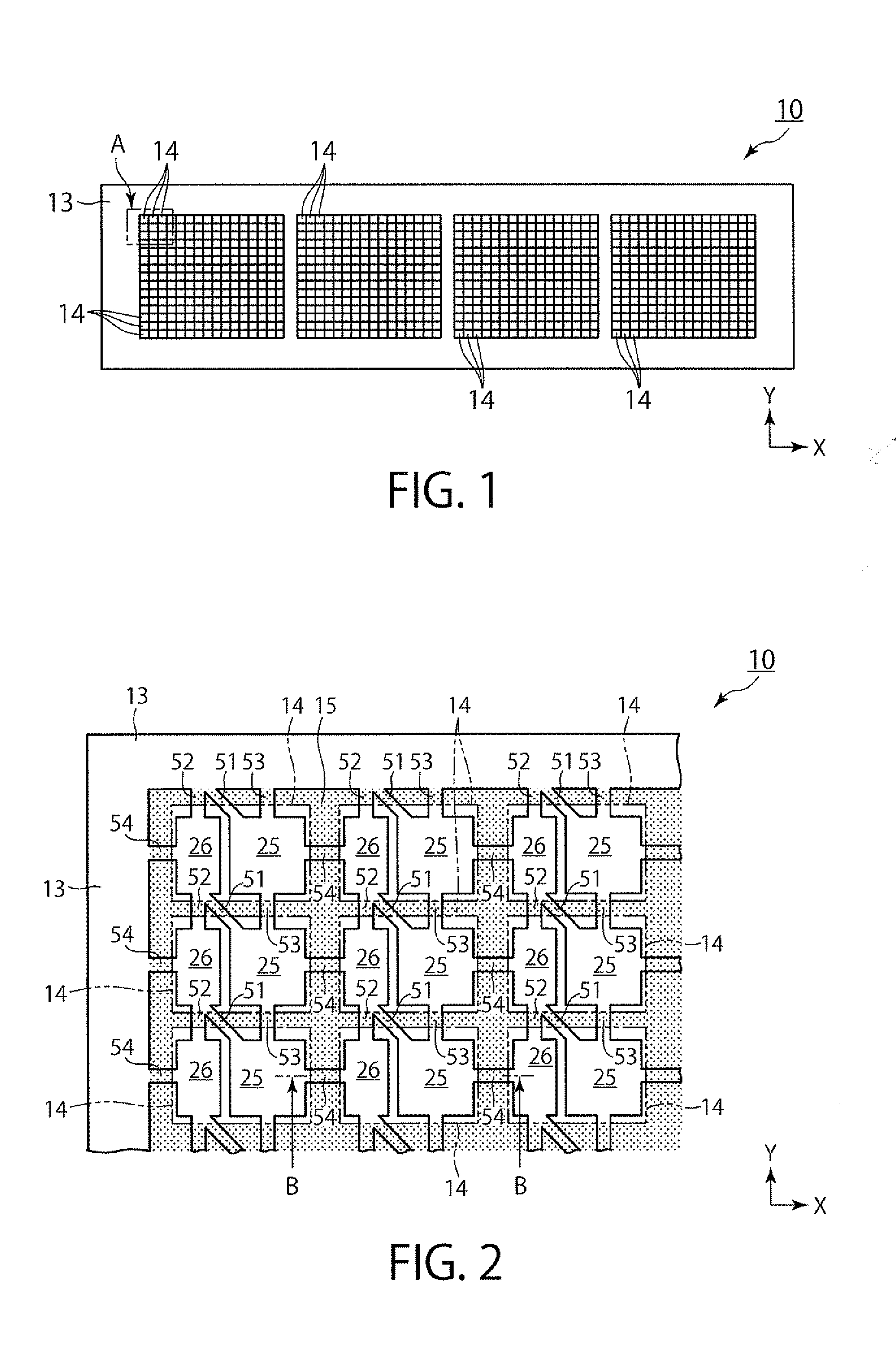
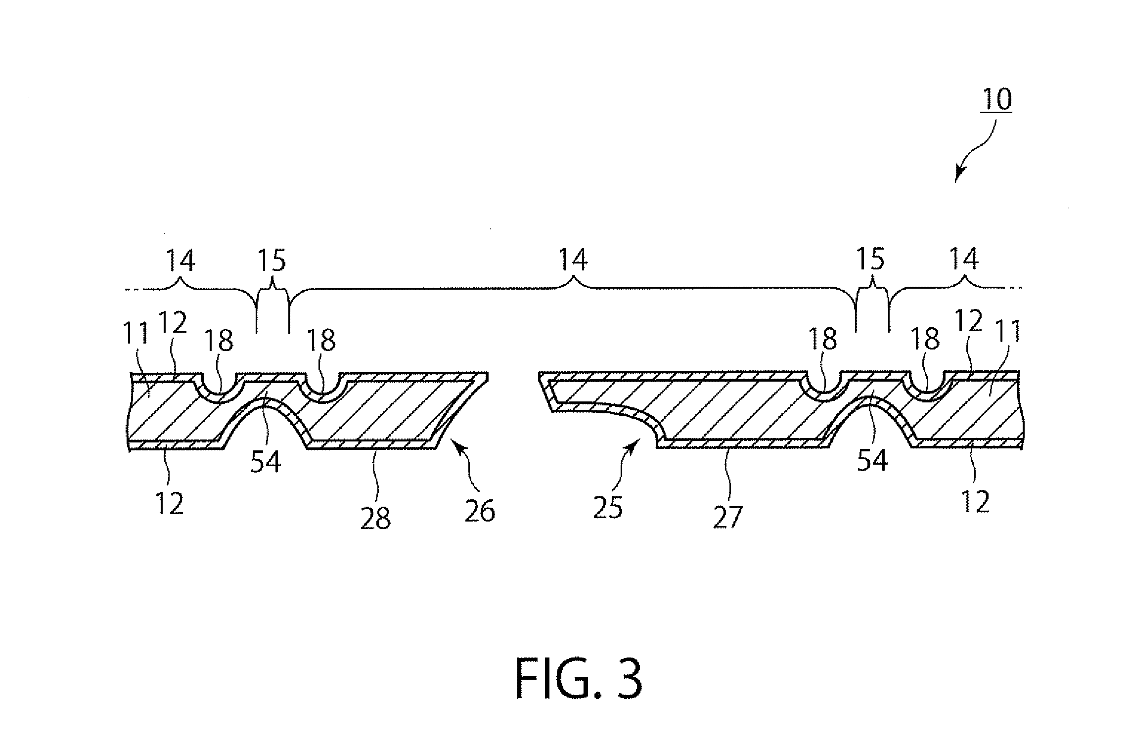
[0094]First, a lead frame for mounting LED elements, according to the present embodiment, is outlined below per FIGS. 1 to 3. FIG. 1 is an overall plan view of the lead frame according to the present embodiment, FIG. 2 is an enlarged view of section A shown in FIG. 1, and FIG. 3 is a sectional view taken along line B-B in FIG. 2.
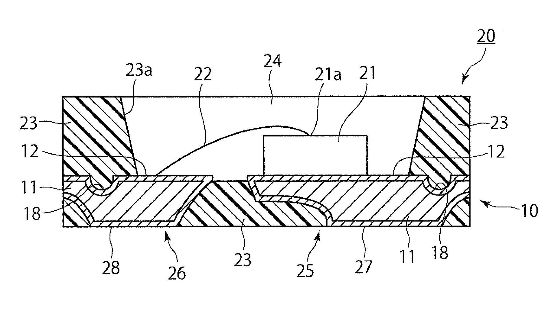
[0095]The lead frame 10 shown in FIG. 1 is used to fabricate semiconductor devices 20 each having an LED element 21 mounted thereupon, one of the semiconductor devices 20 being shown in FIGS. 4 and 5. The lead frame 10 includes a frame body region 13 having an outline of a rectangular shape, and a large number of package regions 14 arranged in multiple rows a...
modification b
[0180]FIG. 19 shows a semiconductor device 20B according to another modification (lens-fitted batch-molded type) of the present embodiment. In the semiconductor device 20B of FIG. 19, a reflecting resin 23 is placed between a die pad 25 and a lead section 26. Unlike that of the semiconductor device 20 shown in FIGS. 4 and 5, however, the reflecting resin 23 is not provided on a lead frame 10.
[0181]Additionally, in FIG. 19, an LED element 21 is connected to a lead frame 10 via solder balls (electroconductive portions) 41a and 41b, instead of a bonding wire 22. That is to say, one of the solder balls 41a, 41b is connected to the die pad 25 and the other solder ball is connected to the lead section 26. Furthermore, in FIG. 19, a dome-shaped lens 61 is formed on an upper surface of a sealing resin 24, to control an irradiating direction of light from the LED element 21.
modification c
[0182]FIG. 20 shows a semiconductor device 20C according to yet another modification (batch-molded type) of the present embodiment. In the semiconductor device 20C of FIG. 20, an LED element 21 and a bonding wire 22 are simultaneously sealed together by a sealing resin 24 only, without using the reflecting resin 23. The sealing resin 24 is also placed between a die pad 25 and a lead section 26, to fill a spatial gap therebetween.
PUM
 Abstract
Description
Claims
Application Information
 - R&D
- Intellectual Property
- Life Sciences
- Materials
- Tech Scout
- Unparalleled Data Quality
- Higher Quality Content
- 60% Fewer Hallucinations
Browse by: Latest US Patents, China's latest patents, Technical Efficacy Thesaurus, Application Domain, Technology Topic, Popular Technical Reports.
© 2025 PatSnap. All rights reserved.Legal|Privacy policy|Modern Slavery Act Transparency Statement|Sitemap|About US| Contact US: help@patsnap.com