Probe assembly

a technology of probes and assembly parts, applied in the field of probe cards, can solve the problems of difficult deformation of thin plate-shaped probes, and achieve the effects of not easy deformation, easy formation of guide grooves, and easy deformation of guide grooves

Inactive Publication Date: 2013-09-12
KIMOTO GUNSEI
View PDF6 Cites 0 Cited by
  • Summary
  • Abstract
  • Description
  • Claims
  • Application Information

AI Technical Summary

Benefits of technology

[0010]In order to overcome the problems described above, the present invention is a probe assembly including: a vertical probe which is formed by etching metal foil, and touches a to-be-inspected semiconductor chip electrode; an output terminal which projects from a side opposite to the side of the vertical probe and touches a wiring board; and a thin plate-shaped probe which has a substantially rectangular cross section at a part thereof and includes an opening which engages a support rod, wherein the support rod includes a first guide groove which guides the opening, a second guide groove which guides the vertical probe, and a third guide groove which guides the output terminal. This structure has an effect that, since the probes constitute a probe assembly, even thin plate-shaped probes are not easily deformed due to buckling, twisting or other causes.
[0011]In an aspect of the present invention, a projection is provided on a side of the vertical probe which faces a guide groove thereof and a projection is provided on a side of the output terminal which faces a guide groove thereof; the projection of the vertical probe is placed in the guide groove thereof and the projection of the output terminal is placed in the guide groove thereof; and phase difference is provided between relative positions of the projections of adjoining vertical probes and between the relative positions of the projections of adjoining output terminals. It is therefore possible to form the guide grooves easily even in fine pitch arrangements.
[0012]In another aspect of the present invention, the Z direction length of the guide groove of the vertical probe equals to the sum total of at least a displacement amount of the vertical probe in the Z direction and the Z-direction length of the projection. It is therefore possible to easily form the guide grooves corresponding to adjoining projections.
[0013]With the structures described above, the probe card according to the present invention is, the following probe card used for inspection of semiconductor chips having fine-pitch pad arrangements, such as LCD-driving LSIs: the probe card is capable of touching electrode pads including continuous fine-pitch pads in a precise and reliable manner; and, at the same time, providing a probe card of lower cost.

Problems solved by technology

This structure has an effect that, since the probes constitute a probe assembly, even thin plate-shaped probes are not easily deformed due to buckling, twisting or other causes.

Method used


Image

  • Probe assembly
  • Probe assembly
  • Probe assembly

Examples


first embodiment

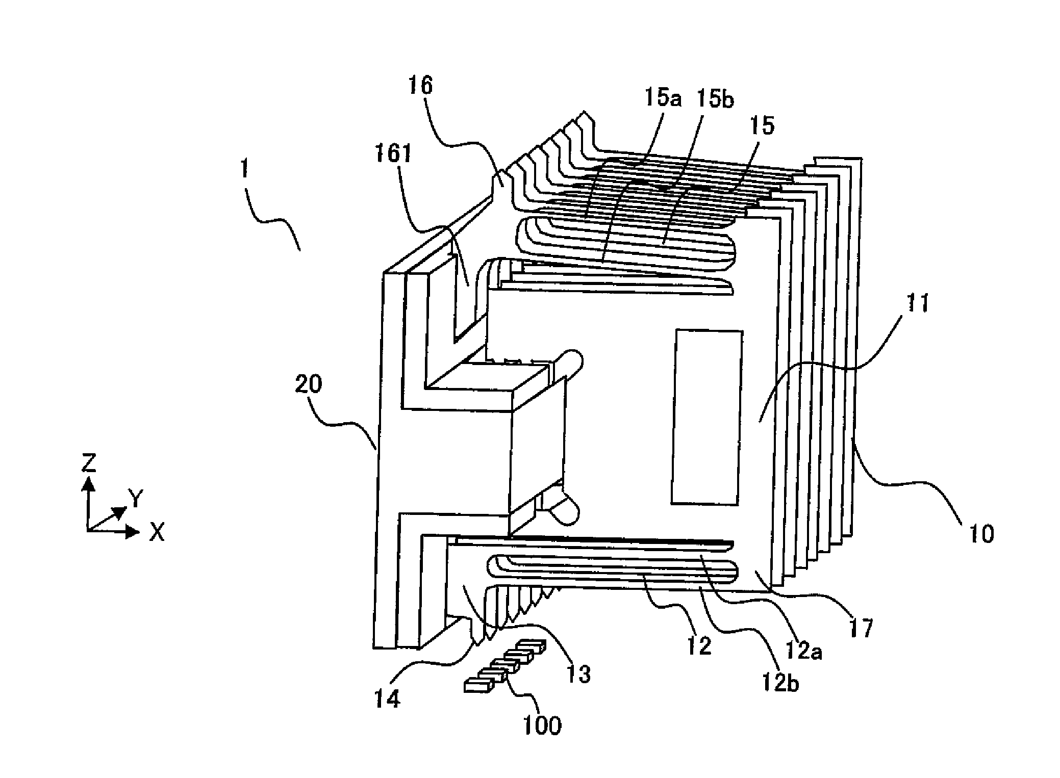
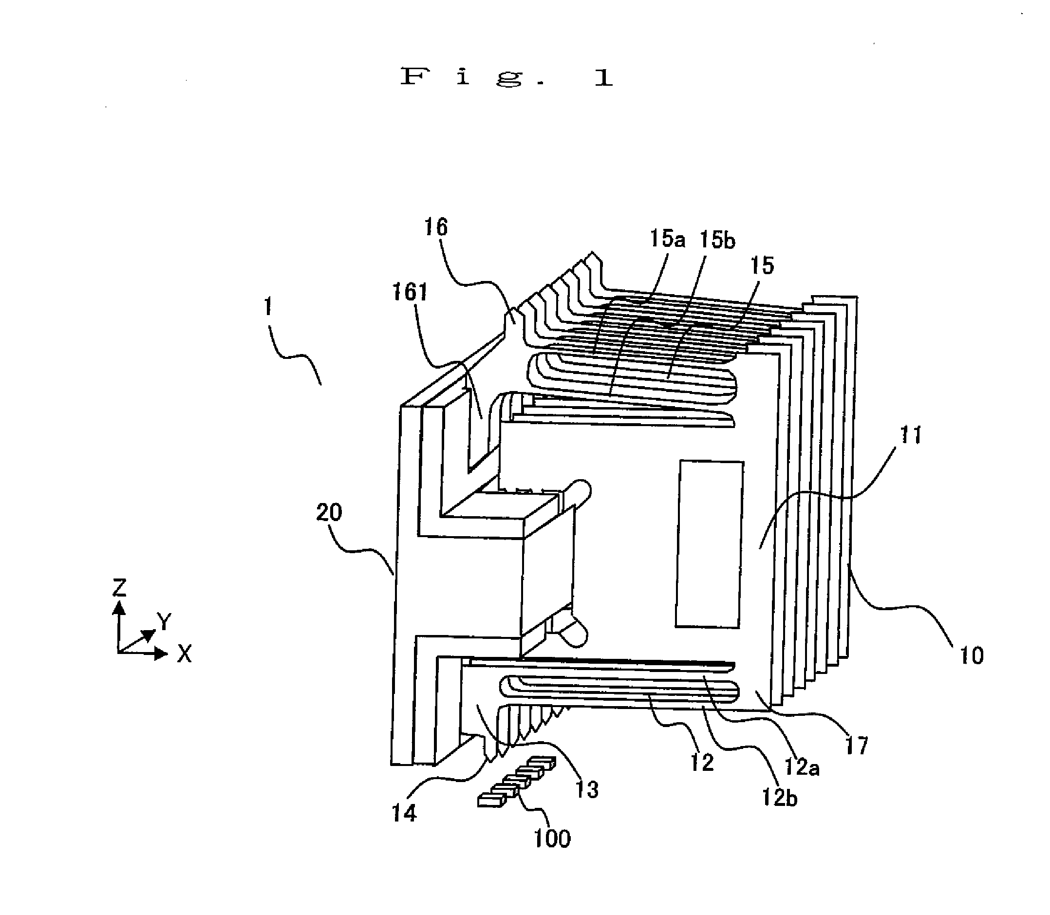
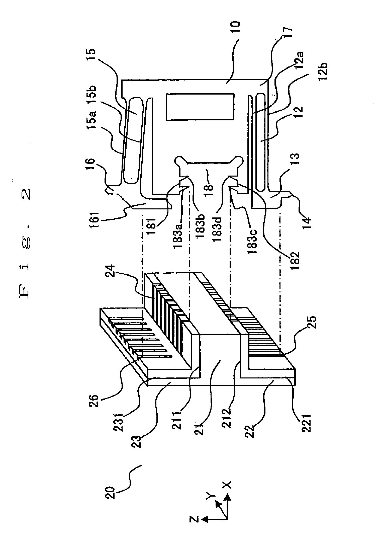
[0024]An embodiment of the present invention will be described in detail with reference to the drawings. FIG. 1 is a perspective view of a first embodiment of the present invention, illustrating an entire structure of a fine-pitch probe assembly. FIGS. 2, 3A and 3B illustrate an operation of the probe assembly.

Probe Structure

[0025]A probe assembly 1 and thin plate-shaped probes 10 which constitute the probe assembly 1 are illustrated in FIGS. 1, 3A and 3B. Each probe 10 includes parallel spring sections 12 and 15 formed by etching metal foil 11. The parallel spring section 12 carries out a probing function. The parallel spring section 15 is formed on the side opposite to that of the parallel spring section 12. Each probe 10 includes an output terminal 16 for the output to a wiring board, and an opening 18 in which a support rod 20 which is a part of the probe assembly 1 is placed and fixed.

[0026]The parallel spring section 12, which touches an electrode pad 100 and carries out a pro...

second embodiment

[0033]Next, a second embodiment of the present invention will be described in detail with reference to the drawings.

Probe Structure

[0034]A thin plate-shaped probe 30 is illustrated in FIGS. 4 to 7B. Each probe 30 includes parallel spring sections 32 and 35 which are formed by etching metal foil 31. The parallel spring section 32 carries a probing function. The parallel spring section 35 is formed on the side opposite to that of the parallel spring section 32. Each probe 30 includes an output terminal 36 for the output to a wiring board, and an opening 38 in which a support rod 40 is placed and fixed.

[0035]The parallel spring section 32, which touches an electrode pad 100 and carries out a probing function, forms a parallelogram spring constituted by a vertical probe 33, two parallel beams 32a and 32b and a fixing section 37. As illustrated in FIG. 7A, when the electrode pad 100 starts touching a tip 34 of the vertical probe 33, and pressing force is increased, spring force is produc...


PUM


Abstract

Provided is a probe assembly that can be used for fine-pitch pads and can be made with lower cost. The probe assembly includes: a vertical probe which is formed by etching metal foil, and touches a to-be-inspected semiconductor chip electrode; an output terminal which projects from a side opposite to the side of the vertical probe and touches a wiring board; a thin plate-shaped probe which has a substantially rectangular cross section at a part thereof and includes an opening which engages a support rod; and a support rod which includes a first guide groove which guides the opening, a second guide groove which guides the vertical probe, and a third guide groove which guides the output terminal.

Description

BACKGROUND OF THE INVENTION[0001]1. Field of the Invention[0002]The present invention relates to a probe card of a prober unit used in a process for manufacturing electronic devices including LSI for inspecting circuits of multiple semiconductor chips that are formed on a semiconductor wafer. More particularly, the present invention relates to a probe card used in a wafer-level probing test. In the probing test, probes are made to touch circuit terminals (“pads”) arranged on the semiconductor chips to perform collective measurement of electrical conductivity of the semiconductor chips.[0003]2. Description of Prior Art[0004]With the advance of semiconductor technology, integration of electronic devices is increasing and the number of electrode terminals (“pads”) formed on each semiconductor chip is also increasing. Then, finer pad arrangements are becoming predominant with, for example, reduced pad areas and finer pad pitches.[0005]Today, the LSI having the finest pitches and the lar...

Claims


Application Information

Patent Timeline
Patent Type & Authority Applications(United States)
IPC IPC(8): G01D21/00
CPCG01R1/07357G01R1/07314
Inventor KIMOTO, GUNSEI
Owner KIMOTO GUNSEI
Why Eureka
Try Eureka