Automated hybrid metrology for semiconductor device fabrication

a hybrid metrology and semiconductor technology, applied in semiconductor/solid-state device testing/measurement, instruments, photomechanical equipment, etc., can solve the problems of reducing yield, obtaining highly accurate measurements, and reducing the accuracy of wafer testing and/or reducing yield

Active Publication Date: 2013-09-19
GLOBALFOUNDRIES US INC +1
View PDF7 Cites 23 Cited by
  • Summary
  • Abstract
  • Description
  • Claims
  • Application Information

AI Technical Summary

Benefits of technology

[0006]This summary is provided, to introduce a selection of concepts in a simplified form that are further described below in the detailed description. This summary is not intended to identify key features or essential features of the claimed subject matter, nor is it intended to be used as an aid in determining the scope of the claimed subject matter.

Problems solved by technology

As a result, devices may be fabricated with features that deviate from their specified physical dimensions, which, in turn, could lead to failures at wafer test and / or reduce yield.
However, obtaining highly accurate measurements typically takes an undesirably long amount of time or involves destructive metrologies which reduce yield.
At the same time, non-destructive measurement tools may be limited in their ability to accurately measure all of the physical features, critical dimensions, and profile information of a device, which, in turn, limits the ability of the foundry (or fab) to maximize yield.

Method used


Image

  • Automated hybrid metrology for semiconductor device fabrication
  • Automated hybrid metrology for semiconductor device fabrication
  • Automated hybrid metrology for semiconductor device fabrication

Examples


Embodiment Construction

[0011]The following detailed description is merely illustrative in nature and is not intended to limit the embodiments of the subject matter or the application and uses of such embodiments. As used herein, the word “exemplary” means “serving as an example, instance, or illustration.” Any implementation described herein as exemplary is not necessarily to be construed as preferred or advantageous over other implementations. Furthermore, there is no intention to be bound by any expressed or implied theory presented in the preceding technical field, background, brief summary or the following detailed description.

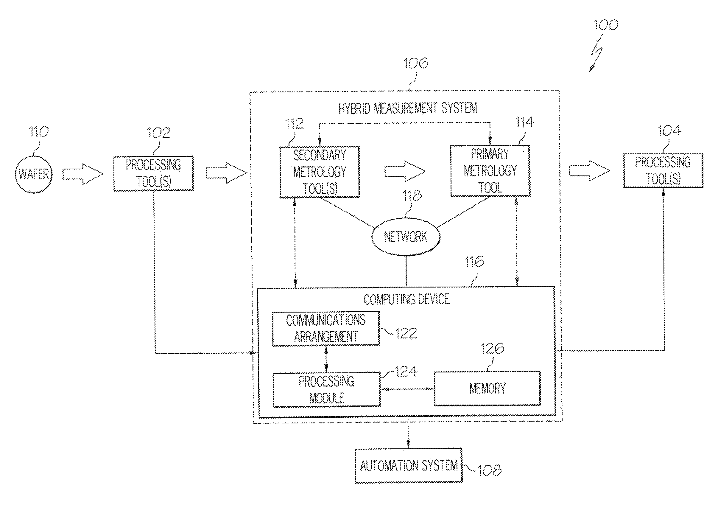
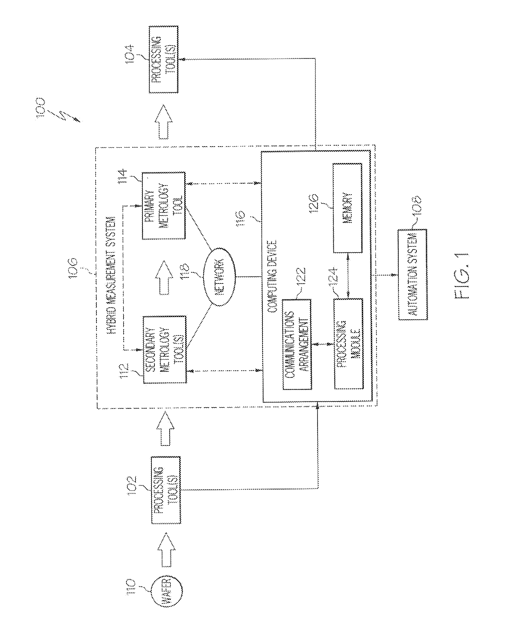
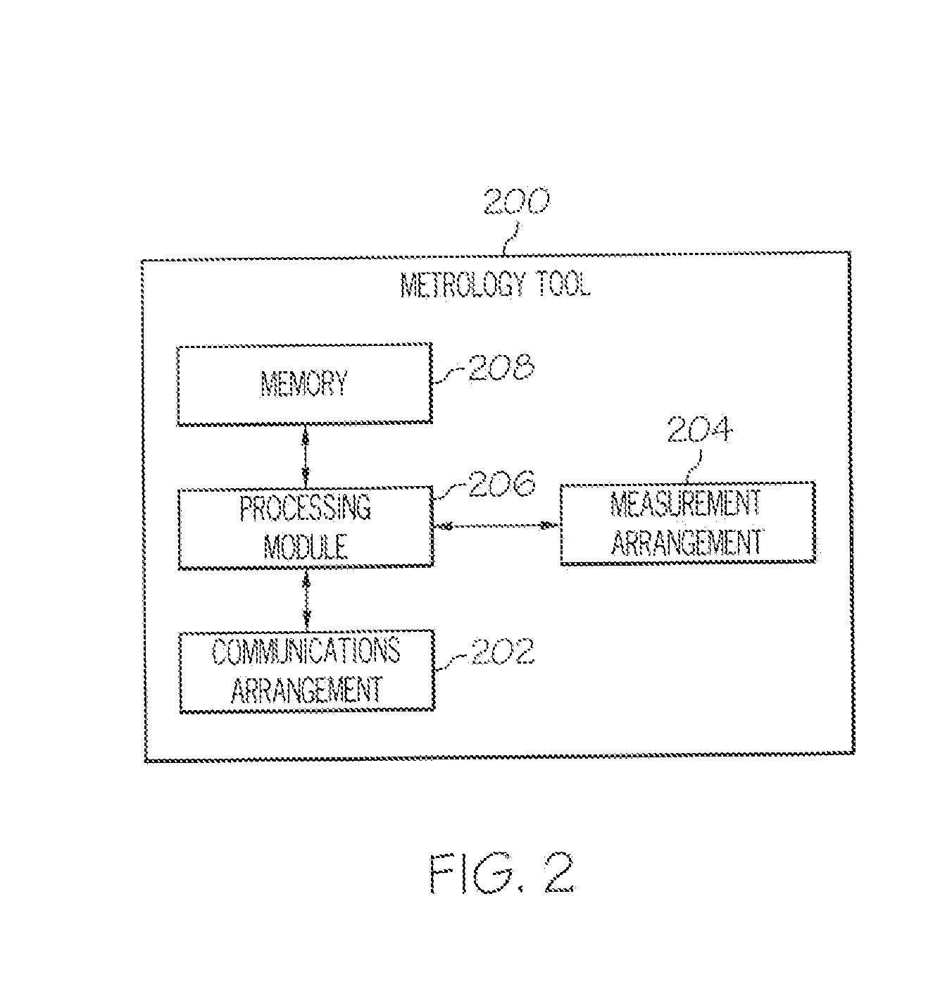
[0012]Embodiments of the subject matter described herein relate to determining hybrid (or composite) measurements of features of semiconductor device structures fabricated on a semiconductor substrate using measurements obtained from different metrology tools in an automated manner. Depending on the embodiment, the feature being measured may be a physical feature, structure or d...


PUM


Abstract

Methods and systems are provided for fabricating and measuring features of a semiconductor device structure. An exemplary method of fabricating a semiconductor device structure involves fabricating a feature of the semiconductor device structure on a wafer of semiconductor material, determining a hybrid recipe for measuring the feature, configuring a plurality of metrology tools to implement the hybrid recipe; and obtaining a hybrid measurement of the feature in accordance with the hybrid recipe.

Description

TECHNICAL FIELD[0001]Embodiments of the subject matter described herein generally relate to semiconductor device structures and related fabrication methods and metrologies, and more particularly, embodiments of the subject matter relate to determining hybrid measurements of physical features, dimensions, or other attributes of a semiconductor device structure using measurements obtained from different metrology tools in an automated manner.BACKGROUND[0002]Semiconductor devices, such as transistors, are the core building block of the vast majority of electronic devices. In practice, it is desirable to accurately and precisely fabricate transistors and other semiconductor devices with physical features having specific physical dimensions, to thereby achieve semiconductor devices having their intended performance characteristics and improve yield. However, the hardware tools used to fabricate the devices may exhibit performance variations. As a result, devices may be fabricated with fe...

Claims


Application Information

Patent Timeline
Patent Type & Authority Applications(United States)
IPC IPC(8): G06F19/00
CPCH01L22/20G03F7/70625H01L22/12
Inventor VAID, ALOKSALEH, NED R.SENDELBACH, MATTHEW J.RANA, NARENDER N.
Owner GLOBALFOUNDRIES US INC
Why Eureka
Try Eureka