Solar cell and method for manufacturing solar cell

a solar cell and solar cell technology, applied in the field of solar cell and method for manufacturing solar cells, can solve problems such as the risk of reducing conversion efficiency, and achieve the effect of improving conversion efficiency and reducing the recombination of minority carriers

Active Publication Date: 2013-09-26
PANASONIC INTELLECTUAL PROPERTY MANAGEMENT CO LTD
View PDF4 Cites 11 Cited by
  • Summary
  • Abstract
  • Description
  • Claims
  • Application Information

AI Technical Summary

Benefits of technology

[0010]An object of an embodiment of the invention is to provide a solar cell in which recombination of minority carriers is reduced and the conversion efficiency is thereby improved, and to provide a method for manufacturing the solar cell.
[0012]In the embodiment, the distance from the endpoint of the second-semiconductor-layer end portion in contact with the rear surface to the second insulating-layer end portion in the arrangement direction is shorter than the distance from the end point to the first insulating-layer end portion in the arrangement direction. This reduces the distance that the minor carriers generated near the first semiconductor layer travel through a portion near a junction between the semiconductor substrate and the second semiconductor layer covered with the insulating layer, when the minor carriers move to the second electrode. Accordingly, in the solar cell of the embodiment, the recombination of minor carries under the second semiconductor layer can be reduced compared to a solar cell in which the width of the insulating layer in the arrangement direction is the same.
[0016]Moreover, the solar cell further comprises an isolation groove for preventing short circuit and, when a semiconductor layer having a p-type conductivity out of the first semiconductor layer formed on the rear surface and the second semiconductor layer formed on the rear surface is defined as a p-type semiconductor layer, a center of the isolation groove is closer to a center of the p-type semiconductor layer than a center of the insulating layer is in the arrangement direction.
[0019]The aspects of embodiments can provide a solar cell in which recombination of minority carriers is reduced and conversion efficiency is thereby improved and provide a method for manufacturing the solar cell.

Problems solved by technology

When the recombination occurs, the number of carriers extracted from electrode 150 decreases and there is a risk of reduction in conversion efficiency.

Method used


Image

  • Solar cell and method for manufacturing solar cell
  • Solar cell and method for manufacturing solar cell
  • Solar cell and method for manufacturing solar cell

Examples


Embodiment Construction

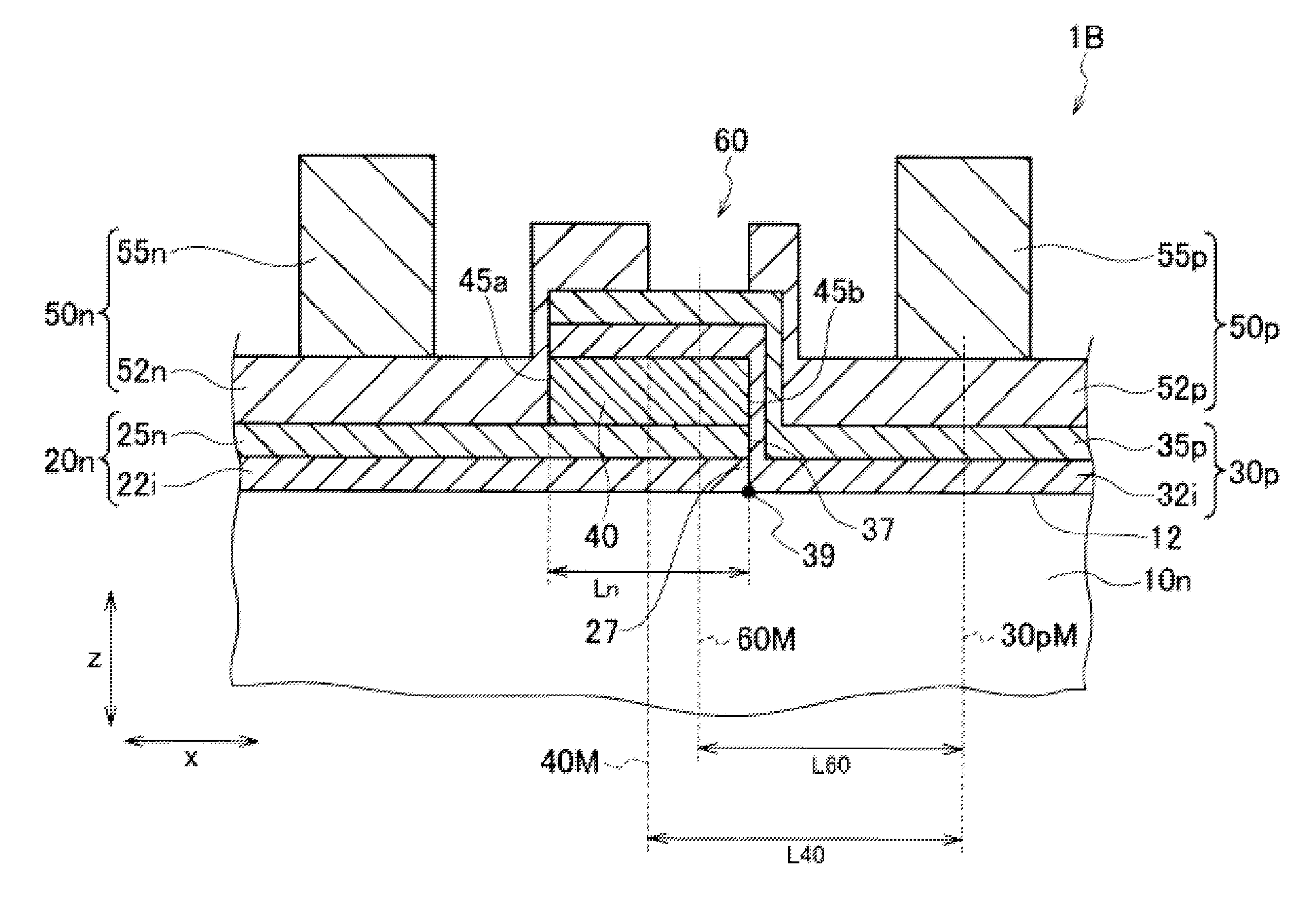
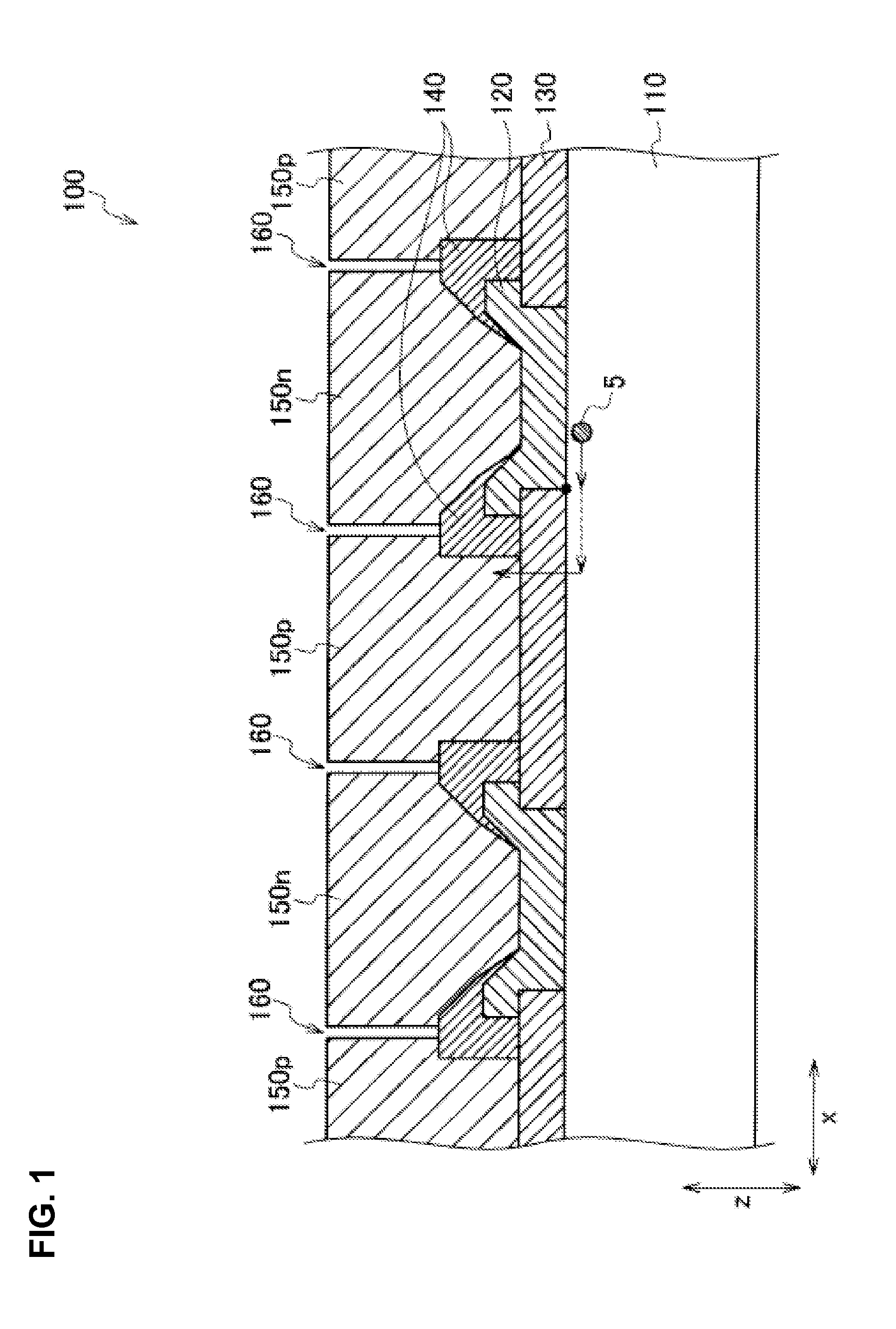
[0034]An example of solar cell 1 according to an embodiment of the invention is described with reference to the drawings. In the drawings described below, the same or similar parts are denoted by the same or similar reference numerals. Note that the drawings are schematic and proportions of dimensions and the like are different from actual ones. Accordingly, specific dimensions and the like should be determined in consideration of the descriptions below. Moreover, parts where relations and proportions of the dimensions are different among the drawings are included as a matter of course.

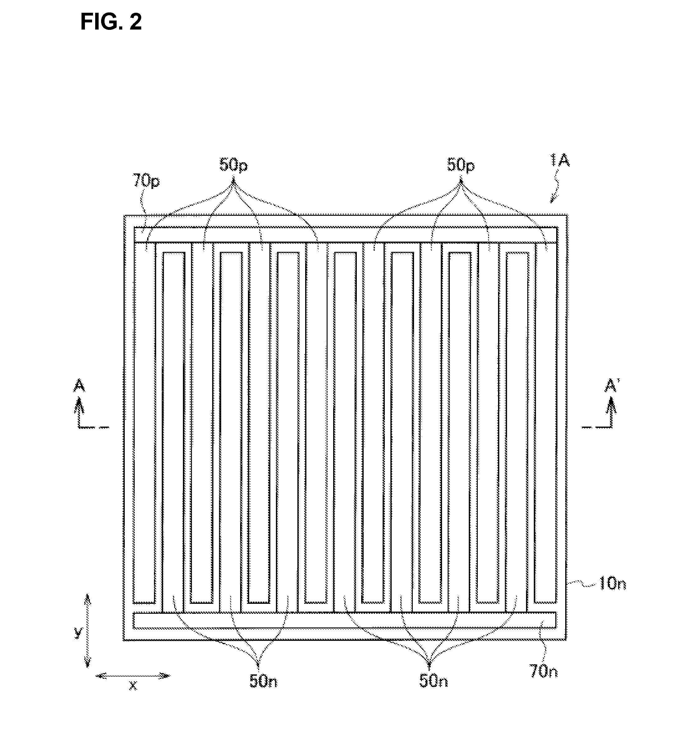
(1) Overall Configuration of Solar Cell 1A

[0035]An overall configuration of solar cell 1A according to the embodiment of the invention is described with reference to FIGS. 2 and 3. FIG. 2 is a plan view of solar cell 1A according to the embodiment of the invention which is viewed from a rear surface 12 side. FIG. 3 is a cross-sectional view taken along the line A-A′ in FIG. 2.

[0036]As shown in FIGS. 2...


PUM


Abstract

A solar cell includes semiconductor substrate of a first conductivity type; first semiconductor layer having a first conductivity type; second semiconductor layer having a second conductivity type; first electrode; second electrode; and insulating layer. First semiconductor layer and second semiconductor layer are formed on rear surface. When one end portion of insulating layer which is formed on first semiconductor layer and which is on a side close to first electrode is defined as first insulating-layer end portion and another end portion of insulating layer on a side close to second electrode is defined as second insulating-layer end portion in arrangement direction x, a distance from end point of second-semiconductor-layer end portion in contact with rear surface to second insulating-layer end portion in arrangement direction x is shorter than a distance from end point to first insulating-layer end portion in arrangement direction x.

Description

CROSS REFERENCE TO RELATED APPLICATIONS[0001]This application is a continuation application of International Application No. PCT / JP2011 / 054310, filed on Feb. 25, 2011, entitled “SOLAR CELL AND METHOD FOR MANUFACTURING SOLAR CELL”, which claims priority based on Article 8 of Patent Cooperation Treaty from prior Japanese Patent Applications No. 2010-042330, filed on Feb. 26, 2010, the entire contents of which are incorporated herein by reference.BACKGROUND OF THE INVENTION[0002]1. Field of the Invention[0003]This disclosure relates to a solar cell of a rear junction type in which an n-type semiconductor layer and a p-type semiconductor layer are formed on a rear surface of a semiconductor substrate and also relates to a method for manufacturing the solar cell.[0004]2. Description of Related Art[0005]A solar cell can convert clean and unlimitedly-supplied solar energy directly into electric energy and is therefore expected to be a new energy source.[0006]A solar cell in which an n-type...

Claims


Application Information

Patent Timeline
Patent Type & Authority Applications(United States)
IPC IPC(8): H01L31/0224H01L31/18
CPCH01L31/022441H01L31/0682Y02E10/547H01L31/1884H01L31/0747H01L31/1804Y02P70/50
Inventor MORIGAMI, MITSUAKIHISHIDA, YUJIIDE, DAISUKESAKATA, HITOSHIMISHIMA, TAKAHIROMORI, HIROYUKISHIGEMATSU, MASATO
Owner PANASONIC INTELLECTUAL PROPERTY MANAGEMENT CO LTD
Why Eureka
Try Eureka