
Container for storing semiconductor device

a technology for semiconductor devices and containers, applied in the field of containers, can solve the problems of high integrated density semiconductor devices, high temperature of semiconductor devices, and high temperature of semiconductor devices, and achieve the effects of preventing contamination, reducing friction between fasteners and drivers, and reducing contact area

Inactive Publication Date: 2013-09-26
GUDENG PRECISION IND CO LTD
View PDF2 Cites 4 Cited by
  • Summary
  • Abstract
  • Description
  • Claims
  • Application Information

AI Technical Summary

Benefits of technology

The present invention relates to a container for storing semiconductor devices. The container includes a fastening member with a fastener and a driver. The fastener is mounted with a rolling element in contact with the driver. This design reduces contact area between the fastener and driver, minimizing friction and preventing production of contaminants. The result is a highly clean container that protects the semiconductor devices during storage. The rolling element moves along with rotation of the driver, effectively reducing friction between the fastener and driver. This ensures that the fastening member works well and the container can be opened and closed smoothly.

Problems solved by technology

But the semiconductor devices with high integrated density are quite sensitive.
Even a bit of contaminants such as particles, dust, organic materials, gas, volatiles, etc result in defects in the semiconductor devices, or static electricity and a short circuit that damage the semiconductor devices.
However, friction occurs between components of fastening members in the container.
Thus not only operation of the fastening member is unstable but the container is not opened or closed smoothly.
Even some contaminants are produced due to the friction and the semiconductor devices stored in the container get polluted.

Method used


Image

  • Container for storing semiconductor device
  • Container for storing semiconductor device
  • Container for storing semiconductor device

Examples


Embodiment Construction

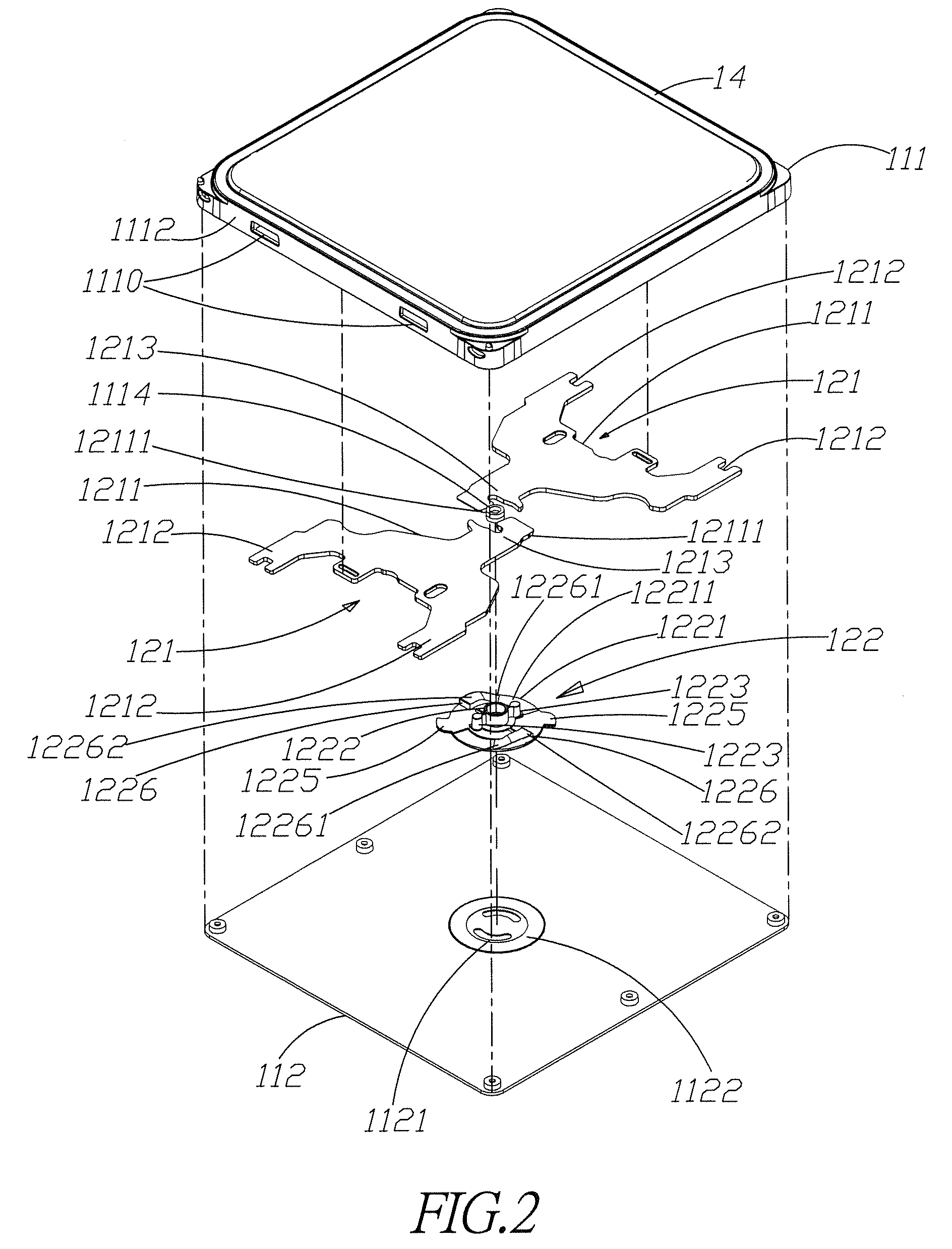
[0021]For solving the problem of friction occurred between each component of the fastening member of the container that cause contamination of semiconductor stored in the container, a container for storing semiconductor devices of the present invention is provided.

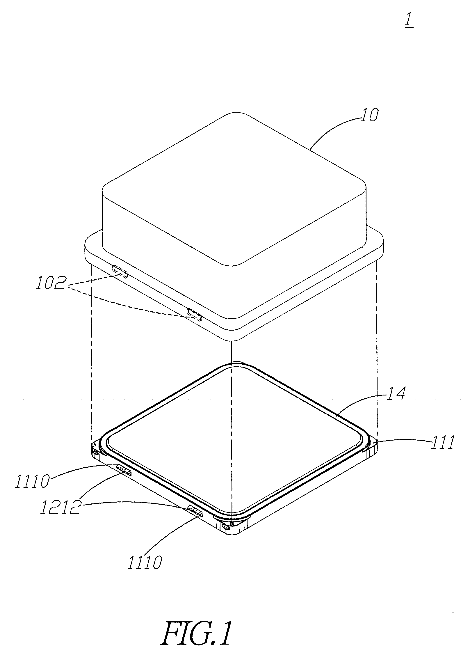
[0022]Refer to FIG. 1, FIG. 2 and FIG. 3, a container for storing semiconductor devices 1 includes a cover 10, a receiving body, and a seal plate 112. At least one semiconductor device is loaded on an outer surface of the receiving body 111 and the cover 10 is disposed over the outer surface of the receiving body 111. The receiving body 111 is mounted with a fastening member therein and the seal plate 112 is against the fastening member for fixing the fastening member in the receiving body 111. The cover 10 is fixed on the receiving body 111 by the fastening member. Thus the container 1 is airtight and is free from external contaminants. Therefore the semiconductor device (such as photomask, wafer or others) will not be po...


PUM


Abstract

A container for storing semiconductor devices is revealed. The container includes a receiving body and a cover. The receiving body is disposed with at least one fastener and at least one driver therein. The fastener includes a rolling element that is in contact with the driver. When the driver is rotated, it drives the fastener to move in the receiving body. At least one fixing part of the fastener is moved toward at least one fastening part of the cover. The cover is fixed on the receiving body by the fixing part locked in the fastening part. Moreover, friction between the fastener and the driver is minimized by the rolling element which reduces contact area between the fastener and the driver so as to prevent production of contaminants in the container and protect semiconductor devices stored in the container from being polluted. Thus the container is of high cleanness.

Description

BACKGROUND OF THE INVENTION[0001]1. Field of the Invention[0002]The present invention relates to a container, especially to a container for storing semiconductor devices.[0003]2. Description of Related Art[0004]Semiconductor chips whose linear width is smaller than 90 nm have been produced in wafer foundries or in semiconductor fabrication plants due to breakthroughs and developments in wafer fabrication techniques. More semiconductor devices per unit wafer are produced along with the minimized linear width and the increased integrated density. But the semiconductor devices with high integrated density are quite sensitive. Even a bit of contaminants such as particles, dust, organic materials, gas, volatiles, etc result in defects in the semiconductor devices, or static electricity and a short circuit that damage the semiconductor devices.[0005]In general manufacturing processes of semiconductor devices, a clean room with a low level of air pollutants is used for protection of the se...

Claims


Application Information

Patent Timeline
Patent Type & Authority Applications(United States)
IPC IPC(8): B65D55/00B65D85/00
CPCH01L21/67373H01L21/67346H01L21/67379H01L21/67383
Inventor KU, CHEN-WEIWANG, SHENG-YUANLEE, CHENG-JU
Owner GUDENG PRECISION IND CO LTD
Features
  • Generate Ideas
  • Intellectual Property
  • Life Sciences
  • Materials
  • Tech Scout
  • Unparalleled Data Quality
  • Higher Quality Content
  • 60% Fewer Hallucinations
Learn More