Non-planar capacitor and method of forming the non-planar capacitor

a non-planar capacitor and capacitor technology, applied in the field of capacitors, can solve the problems of reducing the drive current, increasing the short channel effect, and corresponding increase in short channel effects, and the process currently used to form passive devices, etc., and the capacitors required for many circuit designs are not readily integrated into the process

Active Publication Date: 2013-10-03
GLOBALFOUNDRIES US INC
View PDF2 Cites 17 Cited by
  • Summary
  • Abstract
  • Description
  • Claims
  • Application Information

AI Technical Summary

Benefits of technology

[0005]In view of the foregoing, disclosed herein are embodiments of a non-planar capacitor. This non-planar capacitor can comprise a plurality of fins above a semiconductor substrate. Each fin can comprise at least an insulator section on the semiconductor substrate and a semiconductor section, which has essentially uniform conductivity, stacked above the insulator section. A gate structure can traverse the center portions of the fins. This gate structure can comprise a conformal dielectric layer and a conduc...

Problems solved by technology

For example, size scaling of a single-gate planar field effect transistor resulted in a smaller channel length and, unfortunately, the smaller channel length resulted in a corresponding increase in short channel effects and a dec...

Method used


Image

  • Non-planar capacitor and method of forming the non-planar capacitor
  • Non-planar capacitor and method of forming the non-planar capacitor
  • Non-planar capacitor and method of forming the non-planar capacitor

Examples


Embodiment Construction

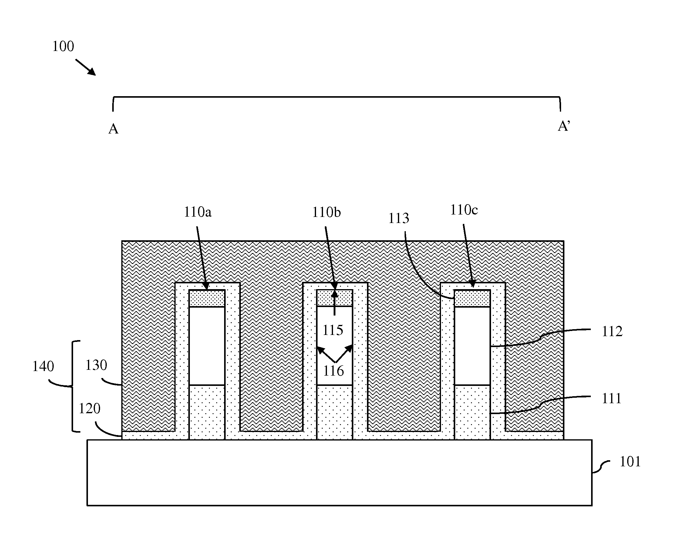
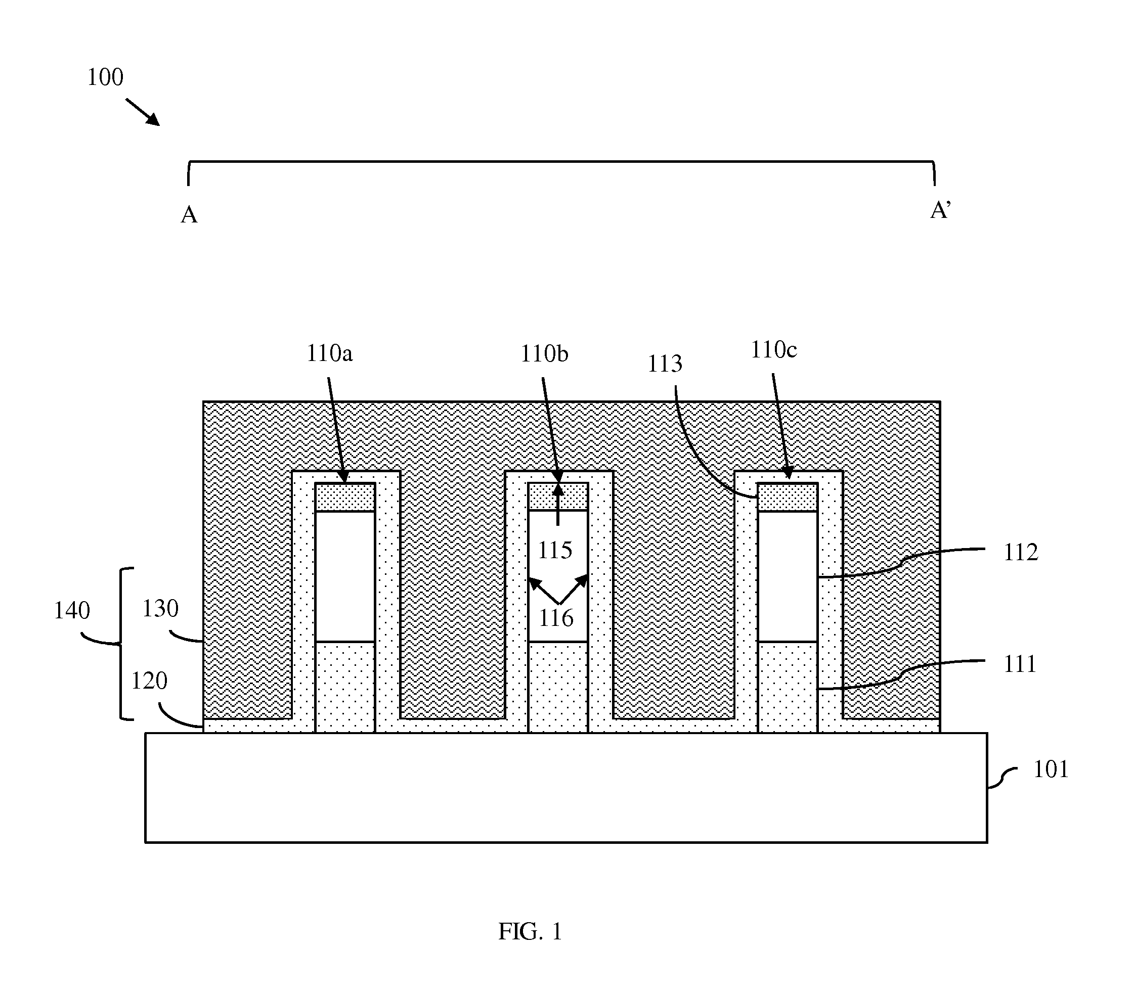
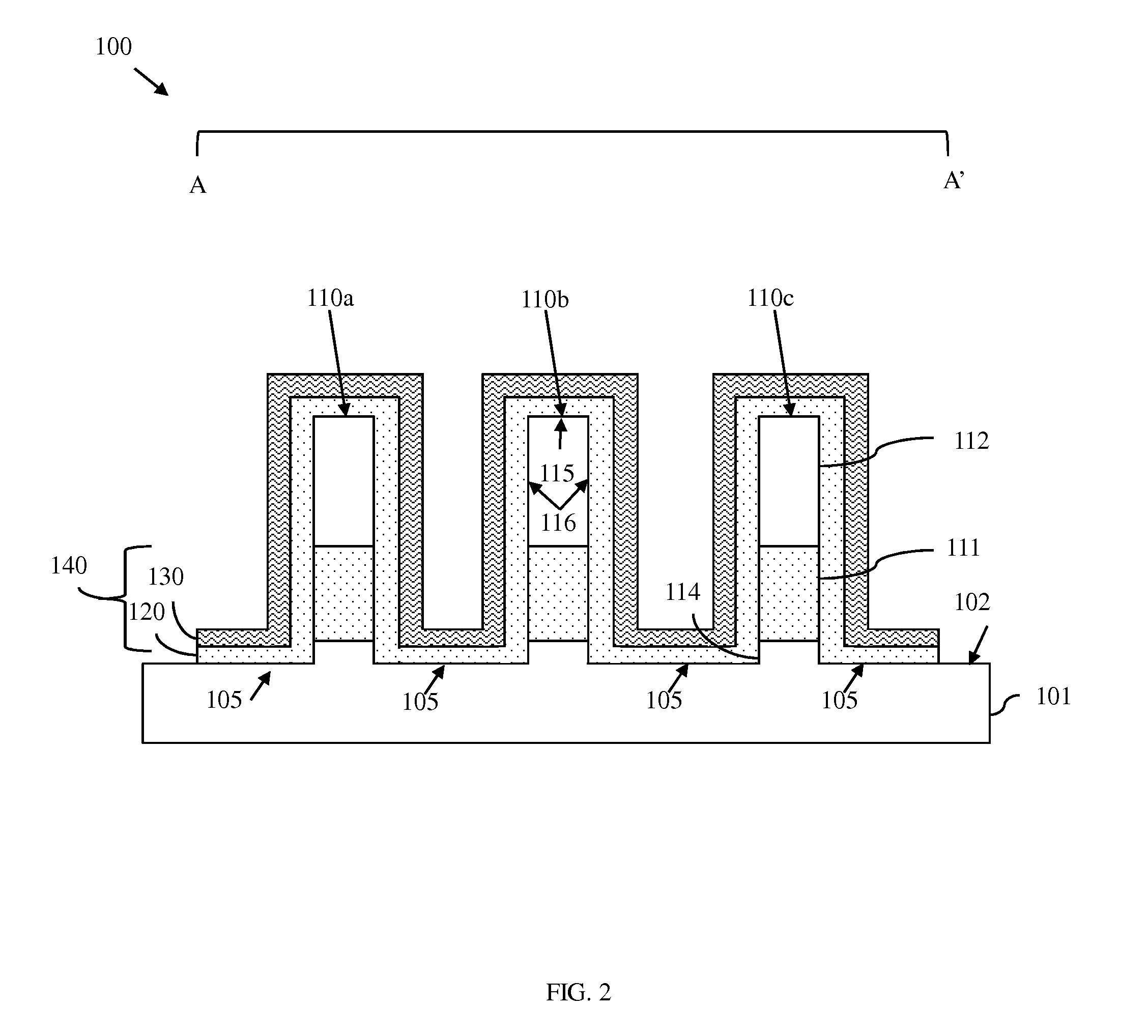
[0040]As mentioned above, integrated circuit design decisions are often driven by device scalability and manufacturing efficiency. For example, size scaling of a single-gate planar field effect transistor resulted in a smaller channel length and, unfortunately, the smaller channel length resulted in a corresponding increase in short channel effects and a decrease in drive current. In response, different types of multi-gate non-planar field effect transistors (MUGFETs), such as dual-gate non-planar FETs (also referred to herein as fin-type FETs (FINFETs)) and tri-gate non-planar FETs, were developed in order to provide reduced-size field effect transistors, while simultaneously avoiding corresponding increases in short channel effects and decreases in drive current.

[0041]Specifically, dual-gate non-planar FETs are non-planar FETs formed using a relatively thin semiconductor fin. For example, the semiconductor fin of a dual-gate non-planar FET can have a height to width ratio of 4:1 o...


PUM


Abstract

Disclosed herein are embodiments of non-planar capacitor. The non-planar capacitor can comprise a plurality of fins above a semiconductor substrate. Each fin can comprise at least an insulator section on the semiconductor substrate and a semiconductor section, which has essentially uniform conductivity, stacked above the insulator section. A gate structure can traverse the center portions of the fins. This gate structure can comprise a conformal dielectric layer and a conductor layer (e.g., a blanket or conformal conductor layer) on the dielectric layer. Such a non-planar capacitor can exhibit a first capacitance, which is optionally tunable, between the conductor layer and the fins and a second capacitance between the conductor layer and the semiconductor substrate. Also disclosed herein are method embodiments, which can be used to form such a non-planar capacitor and which are compatible with current state of the art multi-gate non-planar field effect transistor (MUGFET) processing.

Description

BACKGROUND[0001]1. Field of the Invention[0002]The embodiments disclosed herein relate to capacitors and, more specifically, to a non-planar capacitor structure and to a method of forming the non-planar capacitor.[0003]2. Description of the Related Art[0004]Integrated circuit design decisions are often driven by device scalability and manufacturing efficiency. For example, size scaling of a single-gate planar field effect transistor resulted in a smaller channel length and, unfortunately, the smaller channel length resulted in a corresponding increase in short channel effects and a decrease in drive current. In response, different types of multi-gate non-planar field effect transistors (MUGFETs), such as dual-gate non-planar FETs (also referred to herein as fin-type FETs (FINFETs)) and tri-gate non-planar FETs, were developed in order to provide reduced-size field effect transistors, while simultaneously avoiding corresponding increases in short channel effects and decreases in driv...

Claims


Application Information

Patent Timeline
IPC IPC(8): H01L29/92H01L21/02
CPCH01L21/845H01L27/1211H01L28/90H01L29/94H01L27/0805
Inventor DI SARRO, JAMES P.GAUTHIER, JR., ROBERT J.LEE, TOM C.LI, JUNJUNMITRA, SOUVICKPUTNAM, CHRISTOPHER S.
Owner GLOBALFOUNDRIES US INC
Why Eureka
Try Eureka