Method of epitaxial doped germanium tin alloy formation

Active Publication Date: 2013-10-03
APPLIED MATERIALS INC
View PDF2 Cites 362 Cited by
  • Summary
  • Abstract
  • Description
  • Claims
  • Application Information

AI Technical Summary

Benefits of technology

[0009]Method and apparatus for forming conductive layers on a semiconductor substrate are provided. In one embodiment, a GeSn layer may be selectively formed on semiconductor surfaces of a substrate by positioning a substrate having both dielectric and semiconductor surfaces in a processing chamber, co-flowing a germanium hydride precursor, a tin precursor and a dopant into the processing chamber, epitaxially growing a GeSn layer until the des

Problems solved by technology

As device geometries decline according to Moore's Law, the size of transistor components poses challenges to engineers working to make devices that are smaller, faster, use less power, and generate less heat.
For example, as the size of a transistor declines, the channel

Method used


Image

  • Method of epitaxial doped germanium tin alloy formation
  • Method of epitaxial doped germanium tin alloy formation
  • Method of epitaxial doped germanium tin alloy formation

Examples


Embodiment Construction

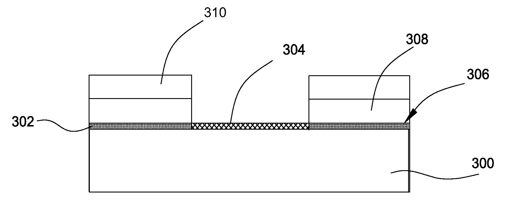
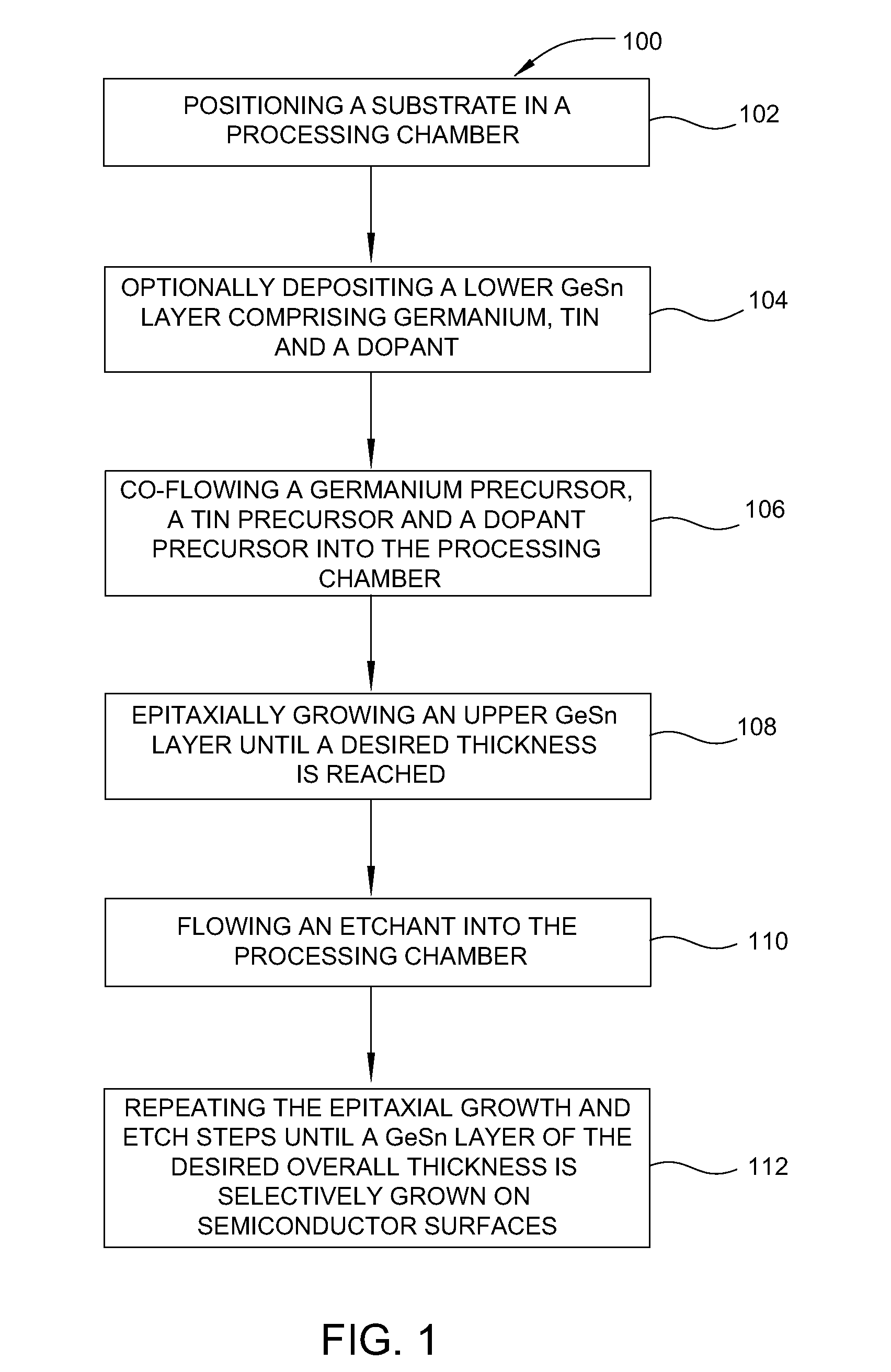
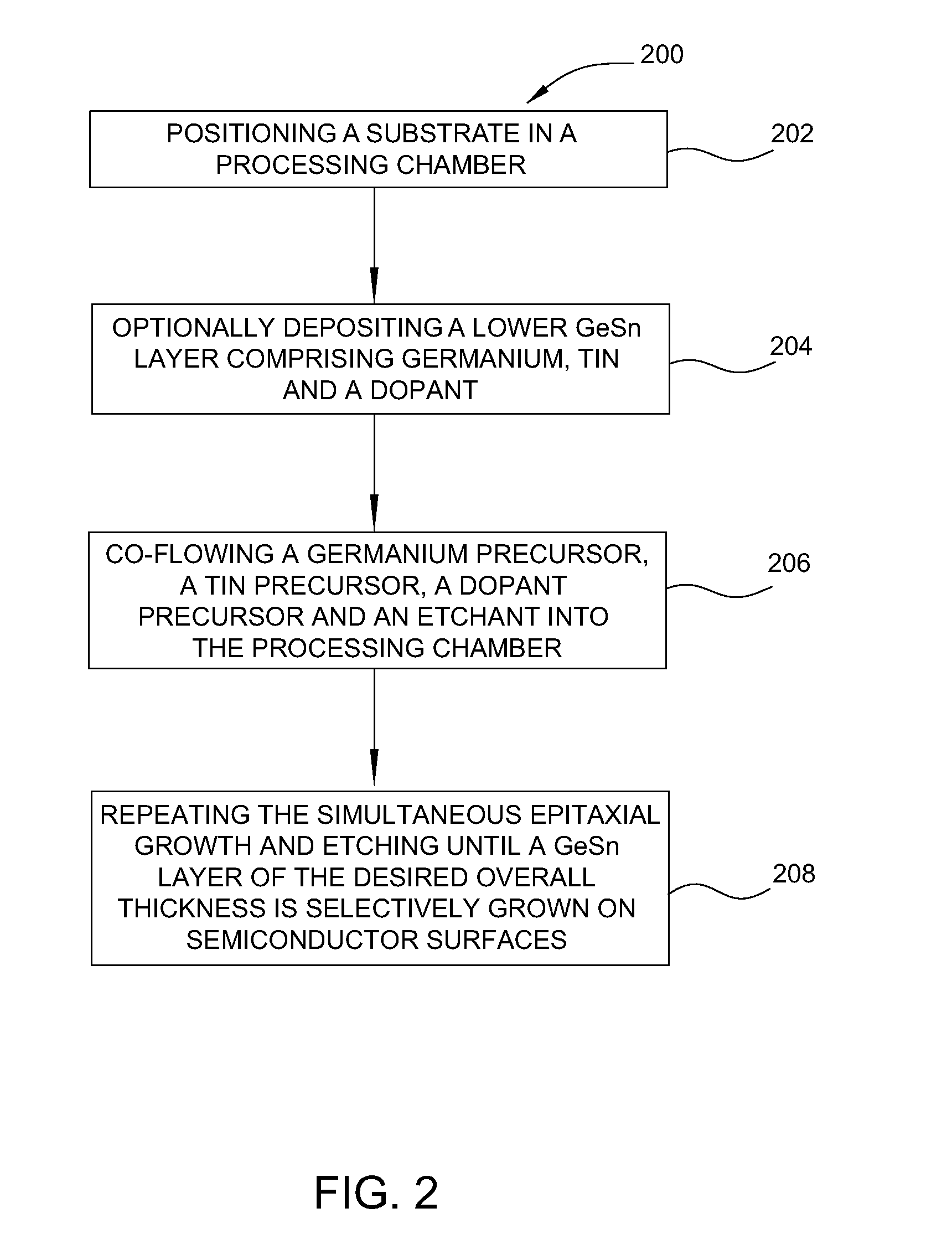
[0018]FIG. 1 is a flow diagram of method 100 according to one or more embodiments. A semiconductor substrate is positioned in a processing chamber at step 102. The semiconductor substrate may be any semiconductive material on which a stressor layer is to be formed, such as silicon or germanium. A silicon substrate on which a transistor structure is to be formed may be used in one example. The silicon substrate may have dielectric areas formed on a surface thereof in some embodiments. For example, the silicon substrate may have transistor gate structures and dielectric spacers formed adjacent to semiconductive source / drain regions, which may be regions of doped silicon or regions on which source / drain materials and contacts are to be formed. Thus, the source / drain regions may comprise the GeSn layers described herein in addition to, or instead of, doped silicon or germanium layers.

[0019]The embodiments described herein typically comprise a GeSn layer which has been doped to control c...


PUM


Abstract

A method for forming germanium tin layers and the resulting embodiments are described. A germanium precursor and a tin precursor are provided to a chamber, and an epitaxial layer of germanium tin is formed on the substrate. The germanium tin layer is selectively deposited on the semiconductor regions of the substrate and can include thickness regions of varying tin and dopant concentrations. The germanium tin layer can be selectively deposited by either alternating or concurrent flow of a halide gas to etch the surface of the substrate.

Description

CROSS-REFERENCE TO RELATED APPLICATIONS[0001]This application claims benefit of U.S. Provisional Patent Application Ser. No. 61 / 619,268 (APPM / 17138L), filed Apr. 2, 2012, which is herein incorporated by reference.BACKGROUND OF THE INVENTION[0002]1. Field of the Invention[0003]Technology described herein relates to manufacture of semiconductor devices. More specifically, methods are described of forming field effect transistors using group IV alloy materials.[0004]2. Description of the Related Art[0005]Germanium was one of the first materials used for CMOS transistors. Due to vast abundance of silicon compared to germanium, however, silicon has been the overwhelming semiconductor material of choice for CMOS manufacture. As device geometries decline according to Moore's Law, the size of transistor components poses challenges to engineers working to make devices that are smaller, faster, use less power, and generate less heat. For example, as the size of a transistor declines, the chan...

Claims


Application Information

Patent Timeline
IPC IPC(8): H01L29/161H01L21/02
CPCH01L29/161H01L21/02535H01L21/02381H01L21/0245H01L21/02452H01L21/0251H01L29/165H01L21/02576H01L21/02579H01L21/0262H01L21/02636H01L29/7848H01L21/02532
Inventor SANCHEZ, ERROL ANTONIO C.HUANG, YI-CHIAU
Owner APPLIED MATERIALS INC
Why Eureka
Try Eureka