Non-boosting program inhibit scheme in NAND design

a technology of inhibiting scheme and boosting program, which is applied in the direction of static storage, digital storage, instruments, etc., to achieve the effect of saving power consumption and low current fn program operation

Inactive Publication Date: 2013-10-17
APLUS FLASH TECH
View PDF7 Cites 64 Cited by
  • Summary
  • Abstract
  • Description
  • Claims
  • Application Information

AI Technical Summary

Benefits of technology

[0010]This invention is fully focusing on the program and program-inhibit operations of NAND cell, NAND cell string and NAND cell array that is employing the HV but extremely low current FN program operation. More particularly, the focus of this invention is to provide a novel approach fo...

Problems solved by technology

Secondly, NAND Flash memory cell design uses a low-current Fowler-...

Method used


Image

  • Non-boosting program inhibit scheme in NAND design
  • Non-boosting program inhibit scheme in NAND design
  • Non-boosting program inhibit scheme in NAND design

Examples


Embodiment Construction

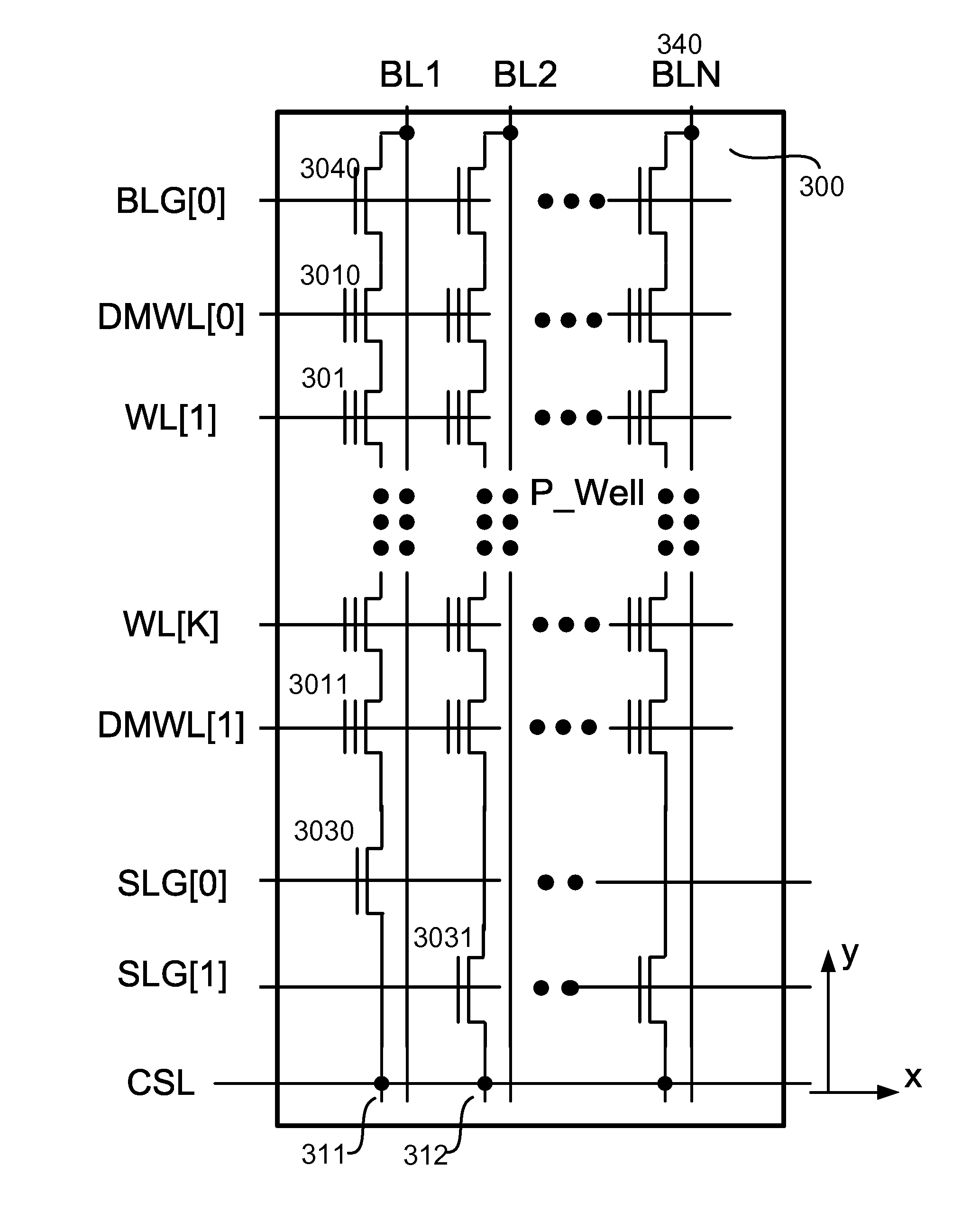
[0052]The present presentation relates to the continuation of improvement over the traditional NAND string and array employed HV Page buffer but extremely low-current FN program operation. More particularly, the present invention relates to a non-boosting program-inhibit scheme to expand current NAND design to HiNAND string and array to achieve more reliable program inhibit operation, though other applications may be recognized on all NVM cells that are using the similar extremely low-current FN-channel erase and FN-channel program.

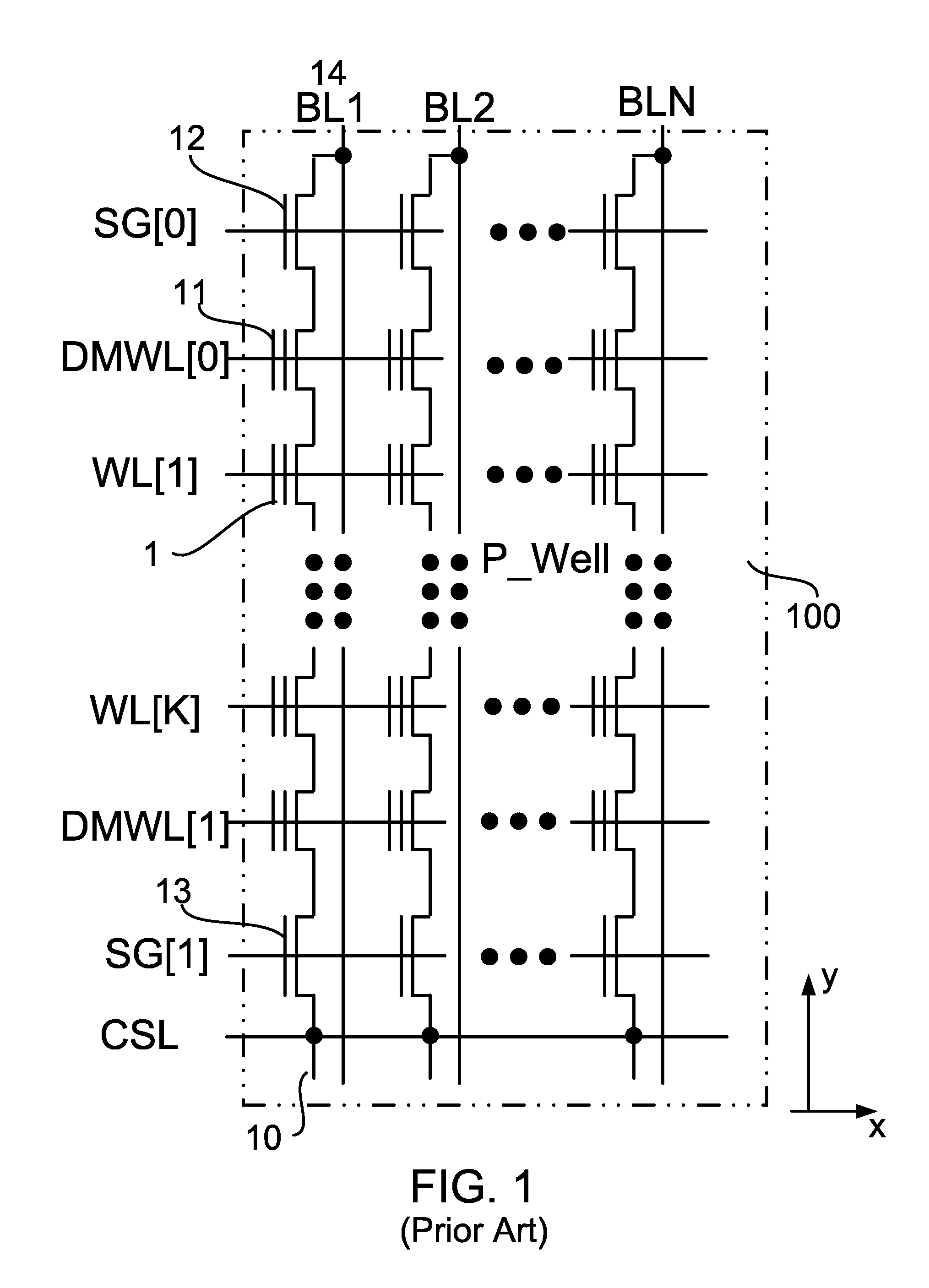
[0053]FIG. 1 is a schematic diagram of a typical NAND flash memory block having N vertical NAND strings according to prior art. Presenting this traditional NAND flash memory block diagram is merely used as part of an inventive process as described below. As seen, each NAND string 10 within the NAND memory block 100 comprises K 2-poly floating-gate NMOS NAND transistors 1 connected in series with a top and a bottom dummy cells 11 (the same 2-poly floating-...


PUM


Abstract

A low-current FN channel scheme for erase, program, program-inhibit and read operations is disclosed for NAND NVM memories. This invention discloses a block array architecture and 3-step half-page program algorithm to achieve less error rate of NAND cell threshold voltage level. Thus, the error correction code capability requirement can be reduced, thus the program yield can be increased to reduce the overall NAND die cost at advanced nodes below 20 nm. As a result, this NAND array can still use the LV, compact PGM buffer for saving in the silicon area and power consumption. In addition, the simpler on-chip state-machine design can be achieved with the superior quality of less program errors.

Description

CROSS-REFERENCES TO RELATED APPLICATIONS[0001]This application claims priority to U.S. Provisional Patent Application No. 61 / 686,805, filed on Apr. 11, 2012, commonly assigned, and hereby incorporated by reference in its entirety herein for all purposes.[0002]This application is related to U.S. patent application Ser. No. 13 / 680,286, filed on Nov. 19, 2012 and PCT Application No. PCT / US2012 / 065734, filed on Nov. 18, 2012, commonly assigned, and hereby incorporated by reference in its entirety herein for all purposes.BACKGROUND OF THE INVENTION[0003]The present invention relates generally to nonvolatile memory technology. More particularly, the present invention relates to a non-boosting program-inhibit scheme used in NAND flash memory design with low-voltage page buffer. Applications of the present invention can be expanded to current NAND design to HiNAND string and array by using a direct, non-boosting scheme to achieve more reliable program-inhibit operation, though more applicat...

Claims


Application Information

Patent Timeline
IPC IPC(8): G11C16/10
CPCG11C16/10G11C16/0483
Inventor LEE, PETER WUNGTSAO, HSING-YA
Owner APLUS FLASH TECH
Why Eureka
Try Eureka