
Programmable LSI

a programmable lsi and semiconductor technology, applied in the direction of power consumption reduction, pulse technique, instruments, etc., can solve the problems of difficult to continue shorten the time necessary, and delay the operation so as to suppress the operation delay suppress the increase in power consumption and circuit area of the programmable lsi, and suppress the effect of the operation delay

Active Publication Date: 2013-10-31
SEMICON ENERGY LAB CO LTD
View PDF19 Cites 52 Cited by
  • Summary
  • Abstract
  • Description
  • Claims
  • Application Information

AI Technical Summary

Benefits of technology

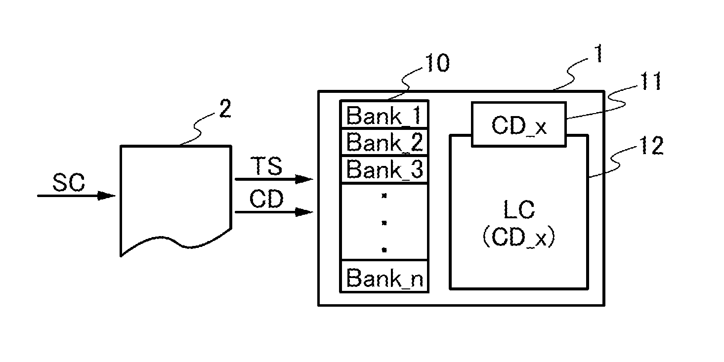
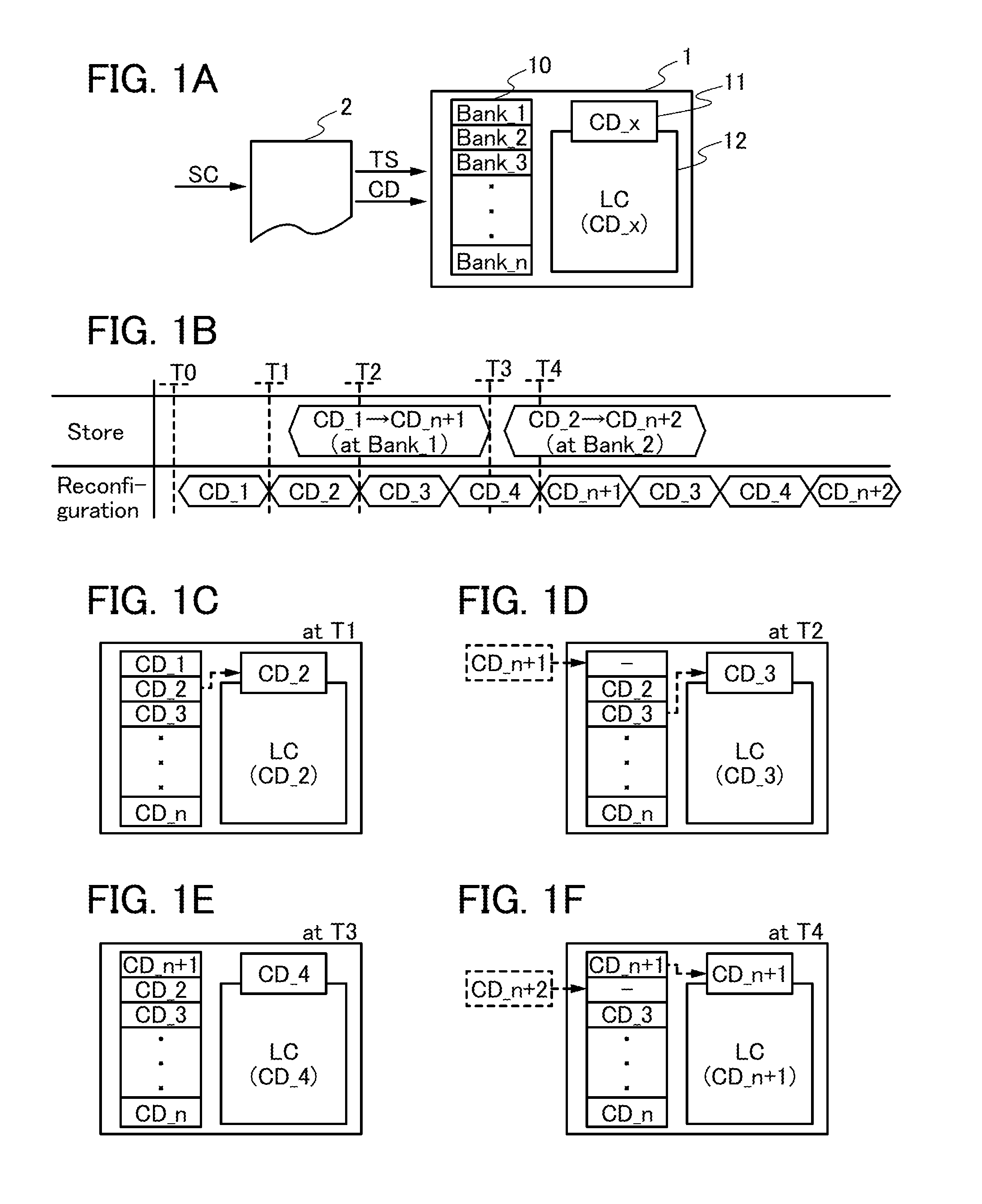
The present invention aims to achieve both suppression of operation delay and reduction in power consumption in a programmable LSI. To achieve this, the programmable LSI is designed to allow for independent and concurrent storage of configuration data and reconfiguration of the logic circuit unit based on the time schedule generated from the source code. This allows for quick rewriting of data in the configuration memory and reduces operation delay of the programmable LSI. Additionally, the programmable LSI can be supplied with required configuration data from the outside as needed, reducing the amount of configuration data needed to be stored and minimizing increased power consumption and circuit area. Overall, the programmable LSI achieves both suppression of operation delay and reduction in power consumption.

Problems solved by technology

In static reconfiguration, the operation of the programmable LSI delays inevitably.
Note that when data in a configuration memory is rewritten with configuration data input from the outside, it is difficult to continue the operation of the programmable LSI.
This is due to design difficulty in sufficiently widening the width of a bus through which data is supplied to the programmable LSI from the outside (difficulty in sufficiently shortening a time necessary for rewriting data in the configuration memory).
However, power consumption of the programmable LSI is inevitably increased because plural pieces of configuration data need to be stored in the DRAM in advance and because refresh operations are required at regular intervals in order to hold the configuration data.
If all pieces of configuration data that may be necessary are stored in a DRAM with the capacity of the DRAM being increased, there occur problems of further increase in power consumption and increase in circuit area.

Method used


Image

  • Programmable LSI
  • Programmable LSI
  • Programmable LSI

Examples


example 1

[0172]A semiconductor device including the programmable LSI of one embodiment of the present invention can be used for display devices, personal computers, and image reproducing devices provided with recording media (typically, devices that reproduce the content of recording media such as digital versatile discs (DVDs) and have displays for displaying the reproduced images). Other examples of a semiconductor device including the programmable LSI of one embodiment of the present invention are mobile phones, game machines including portable game consoles, portable information terminals, e-book readers, cameras such as video cameras and digital still cameras, goggle-type displays (head mounted displays), navigation systems, audio reproducing devices (e.g., car audio systems and digital audio players), copiers, facsimiles, printers, multifunction printers, automated teller machines (ATM), and vending machines.

[0173]The description is made on examples where a semiconductor device includi...


PUM


Abstract

An object is to achieve both suppression of operation delay and reduction in power consumption of a programmable LSI. A compiler generates, from source code, configuration data needed in a programmable LSI and a time schedule that shows a timing of using the data in the programmable LSI (a timing at which the data is held in a configuration memory) and a timing of storing the data in the programmable LSI before the data is used. Supply of new configuration data to the programmable LSI from the outside (storage of new configuration data) and data rewrite in the configuration memory in the programmable LSI (circuit reconfiguration) are performed independently and concurrently on the basis of the time schedule.

Description

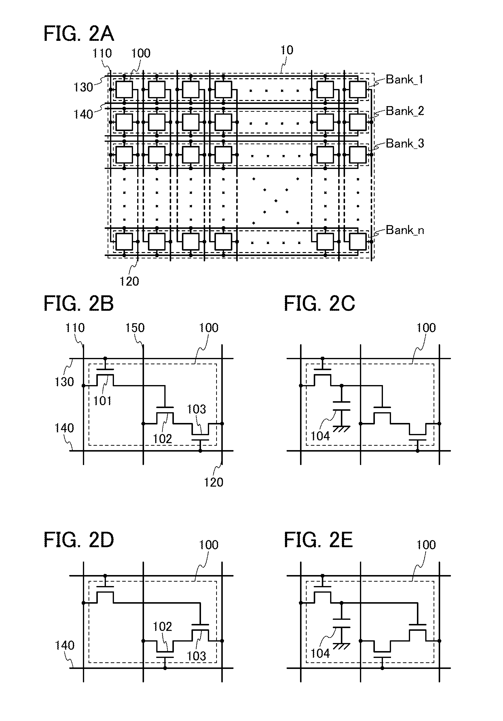
BACKGROUND OF THE INVENTION[0001]1. Field of the Invention[0002]The present invention relates to a programmable LSI and a semiconductor device including the programmable LSI. Note that a semiconductor device in this specification indicates any device that can operate by utilizing semiconductor characteristics. For example, electro-optical devices, semiconductor circuits, and electronic devices are all included in the category of the semiconductor device.[0003]2. Description of the Related Art[0004]Programmable LSIs, which are reconfigurable, have advantages such as reduction in development period and flexibility in changing design specification, as compared to a conventional application specific integrated circuit (ASIC) and gate array, and have been widely used in semiconductor devices.[0005]Specifically, a programmable LSI has a memory (configuration memory) that holds data (configuration data) for setting a circuit configuration. The circuit configuration is determined on the bas...

Claims


Application Information

Patent Timeline
IPC IPC(8): H03K19/00
CPCH03K19/0013H03K19/17784H03K19/17792H03K19/173H03K19/177
Inventor KUROKAWA, YOSHIYUKI
Owner SEMICON ENERGY LAB CO LTD
Learn More