Semiconductor device and driving method thereof

a technology of mikro-onductors and driving methods, applied in logic circuits, pulse techniques, logic circuit coupling/interface arrangements, etc., can solve the problem of not sufficiently revealing a pld in which operation delay is suppressed, and achieve the effect of suppressing operation delay in a pld, suppressing the boosting effect of a charge retention node, and suppressing operation delay

Active Publication Date: 2016-07-05
SEMICON ENERGY LAB CO LTD
View PDF137 Cites 3 Cited by
  • Summary
  • Abstract
  • Description
  • Claims
  • Application Information

AI Technical Summary

Benefits of technology

[0010]In view of the above-described technical background, an object of one embodiment of the present invention is to provide a novel driving method of a semiconductor device. Another object is to provide a novel semiconductor device that enables a novel driving method of a semiconductor device. More specifically, an object of one embodiment of the present invention is to provide a driving method that suppresses operation delay in a PLD. Another object is to provide a novel PLD in which operation delay can be suppressed.
[0031]Furthermore, according to one embodiment of the present invention, operation delay in a PLD can be suppressed in such a manner that a boosting effect of a charge retention node due to capacitive coupling is utilized when dynamic reconfiguration is performed.
[0033]Furthermore, according to one embodiment of the present invention, a novel PLD in which operation delay can be suppressed can be provided.

Problems solved by technology

Patent Document 1 discloses a PLD in which a configuration memory is formed using a nonvolatile memory comprised of a small number of transistors and the area for arranging the configuration memory is reduced; however, it does not sufficiently disclose a PLD in which operation delay is suppressed.

Method used


Image

  • Semiconductor device and driving method thereof
  • Semiconductor device and driving method thereof
  • Semiconductor device and driving method thereof

Examples


embodiment 1

[0053]A semiconductor device and a driving method thereof that are embodiments of the present invention will be described with reference to FIGS. 1 to 4.

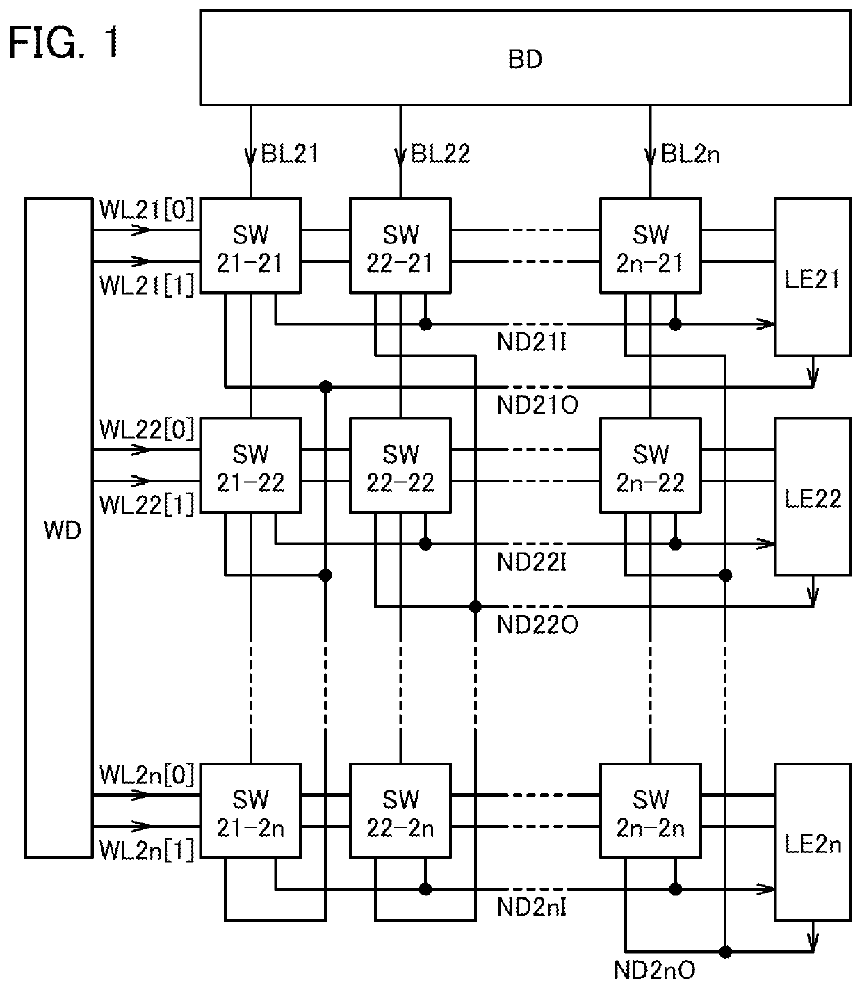
[0054]FIG. 1 shows a circuit structure of a semiconductor device of one embodiment of the present invention.

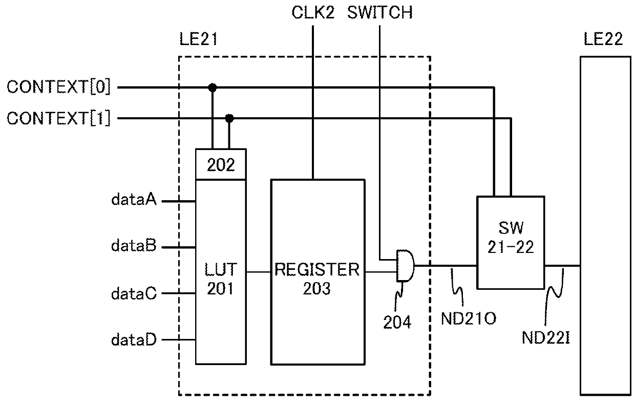
[0055]The PLD shown in FIG. 1 includes n (n is an integer of 2 or more) logic elements LE (logic elements LE21 to LE2n), n2 circuits SW (circuits SW21-21 to SW2n-2n), a bit driver BD, and a word driver WD.

[0056]The logic element LE includes a configuration memory inside, and has a function of outputting a specific output signal with respect to an input signal, in accordance with configuration data stored in the configuration memory.

[0057]The circuit SW has a function of controlling conduction between the logic elements LE. The circuit SW can be expressed as a “switch”, because of the nature of its function. Although a structure in FIG. 1 has n2 circuits SW with respect to n logic elements LE, the present invention is not limit...

embodiment 2

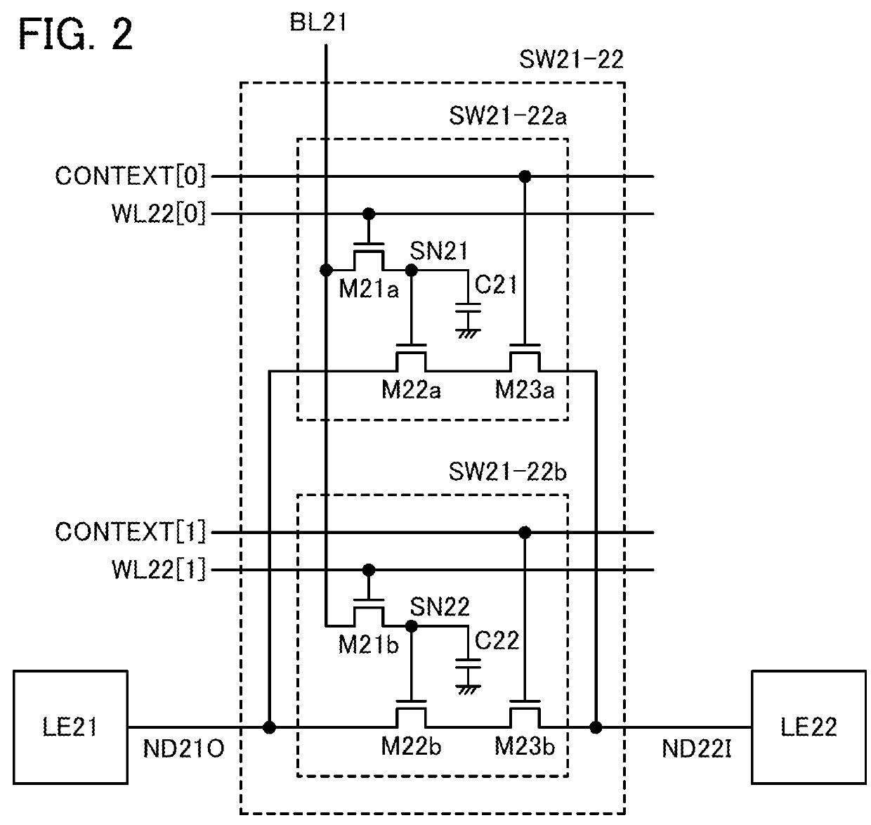
[0083]A semiconductor device and a driving method that are embodiments of the present invention will be described with reference to FIG. 2, FIG. 3, and FIGS. 5 to 7.

[0084]The driving method of a semiconductor device described in this embodiment is the same as the driving method described in Embodiment 1 in that a period in which configuration under favorable conditions is performed is provided. However, the driving method of a semiconductor device described in this embodiment is different from the driving method described in Embodiment 1 in the method of preventing a malfunction caused by data variation of a logic element LE, which should be taken into account when configuration under favorable conditions is performed. Accordingly, this point in particular will be described in detail.

[0085]FIG. 5 shows a circuit structure of a PLD according to one embodiment of the present invention.

[0086]The circuit shown in FIG. 5 is different from the circuit shown in FIG. 1 in that it includes c...

embodiment 3

[0097]A semiconductor device and a driving method that are embodiments of the present invention will be described with reference to FIGS. 13 to 16.

[0098]FIG. 13 shows a circuit structure of a semiconductor device according to one embodiment of the present invention.

[0099]The PLD shown in FIG. 13 includes n (n is an integer of 2 or more) logic elements LE (logic elements LE31 to LE3n), n2 circuits SW (circuits SW31-31 to SW3n-3n), a bit driver BD, a word driver WD, and n circuits ST (circuits ST31 to ST3n).

[0100]The logic element LE includes a configuration memory inside, and has a function of outputting a specific output signal with respect to an input signal, in accordance with configuration data stored in the configuration memory.

[0101]The circuit SW has a function of controlling conduction between the logic elements LE. The circuit SW can be expressed as a “switch”, because of the nature of its function. Although a structure in FIG. 13 has n2 circuits SW with respect to n logic e...


PUM


Abstract

A semiconductor device in which operation delay can be suppressed is provided. The semiconductor device includes a first logic element, a second logic element, a first circuit that has a function of controlling conduction between the first logic element and the second logic element, and a fourth circuit. The fourth circuit is electrically connected to the first circuit, and is electrically connected to the second logic element.

Description

BACKGROUND OF THE INVENTION[0001]1. Field of the Invention[0002]The technical field of one embodiment of the invention disclosed in this specification, drawings, and the like relates to an object, a method, or a manufacturing method. Alternatively, it relates to a process, a machine, manufacture, or a composition of matter. Specifically, one embodiment of the invention relates to a semiconductor device and a driving method thereof. More specifically, one embodiment of the invention relates to a programmable logic device and a driving method thereof.[0003]2. Description of the Related Art[0004]An application specific integrated circuit (ASIC) is a circuit in which all circuits are fixed at the time of manufacture, whereas a programmable logic device (hereinafter also referred to as PLD in this specification) is a device that can function with an intended circuit structure set by a user after the shipment. The PLD described in this specification includes all of the following in its ca...

Claims


Application Information

Patent Timeline
Patent Type & Authority Patents(United States)
IPC IPC(8): H03K19/0185H03K19/0944
CPCH03K19/018507H03K19/0944
Inventor OKAMOTO, YUKIKUROKAWA, YOSHIYUKI
Owner SEMICON ENERGY LAB CO LTD
Why Eureka
Try Eureka