Shift register and semiconductor display device

a technology of shift register and semiconductor display device, which is applied in the direction of instruments, computation using denominational number representation, pulse technique, etc., can solve the problems of increasing the cost occupying a larger area of the internal circuit, and reducing the stability of the semiconductor display device, so as to promote lattice distortion, increase stability, and stable free energy

Active Publication Date: 2009-10-13
SEMICON ENERGY LAB CO LTD
View PDF43 Cites 22 Cited by
  • Summary
  • Abstract
  • Description
  • Claims
  • Application Information

AI Technical Summary

Benefits of technology

[0008]The invention is made in view of the aforementioned problems to provide a shift register which can operate normally while suppressing a delay of signal and a rounding of waveform. Moreover, the invention provides a semiconductor display device which can operate an internal circuit normally while suppressing an area for the internal circuit and suppressing the delay of signal and the rounding of waveform. Further, the invention provides a semiconductor display device which can operate the internal circuit normally while suppressing the size of a housing and increase in cost and power consumption.
[0015]A semi-amorphous semiconductor film is a film including a semiconductor of an intermediate structure between amorphous and crystalline structures (including single crystalline and polycrystalline structures). A semi-amorphous semiconductor is a semiconductor having a third state which is stable in free energy. Moreover, a semi-amorphous semiconductor is a crystalline semiconductor having a short distance order and lattice distortion, and formed by dispersing a grain having a diameter of 0.5 to 20 nm in an amorphous semiconductor. Raman spectrum of a semi-amorphous semiconductor is shifted toward lower wave numbers than 520 cm−1. The diffraction peaks of (111) and (220), which are believed to be derived from Si crystal lattice, are observed in the semi-amorphous semiconductor film by X-ray diffraction. The semi-amorphous semiconductor film contains hydrogen or halogen by at least 1 atom % or more for terminating dangling bonds. Such a semiconductor is called a semi-amorphous semiconductor (SAS) here for convenience. A favorable semi-amorphous semiconductor can be obtained by promoting the lattice distortion by providing a rare gas element such as helium, argon, krypton, and neon to increase stability.
[0016]According to the shift register of the invention, a timing at which a signal outputted from an output terminal of a clocked inverter rises and falls can be controlled by using a signal outputted from two stages before. Accordingly, the shift register can operate normally while suppressing a delay of signal and a rounding of waveform even when an amplitude of a clock inputted to the clocked inverter is smaller than that of a power source voltage.
[0017]Moreover, the transmission gate can control a clock signal input to a flip-flop circuit, therefore, a load imposed on a wiring for supplying the clock signal can be reduced.
[0018]By using the aforementioned shift register in the semiconductor display device of the invention, an internal circuit can normally operate while suppressing an area for the internal circuit and a delay of signal and a rounding of waveform. Moreover, according to the semiconductor display device of the invention, the internal circuit can operate normally while suppressing the size of a housing and increase in cost and power consumption.

Problems solved by technology

In the case of providing a level shifter in the internal circuit for amplifying a signal inputted from the external circuit as described in Patent Document 1, problems occur in that the internal circuit occupies a larger area, a signal is delayed, and a waveform is rounded.
However, when the level shifter is provided in the external circuit for amplifying a signal, a housing has to be formed larger as the number of components for an IC increases, which causes an increase in cost of the semiconductor display device.
When a signal is amplified in the external circuit, a high power source voltage has to be supplied to the external circuit as well, which leads to an increase in power consumption.

Method used


Image

  • Shift register and semiconductor display device
  • Shift register and semiconductor display device
  • Shift register and semiconductor display device

Examples


embodiment mode 1

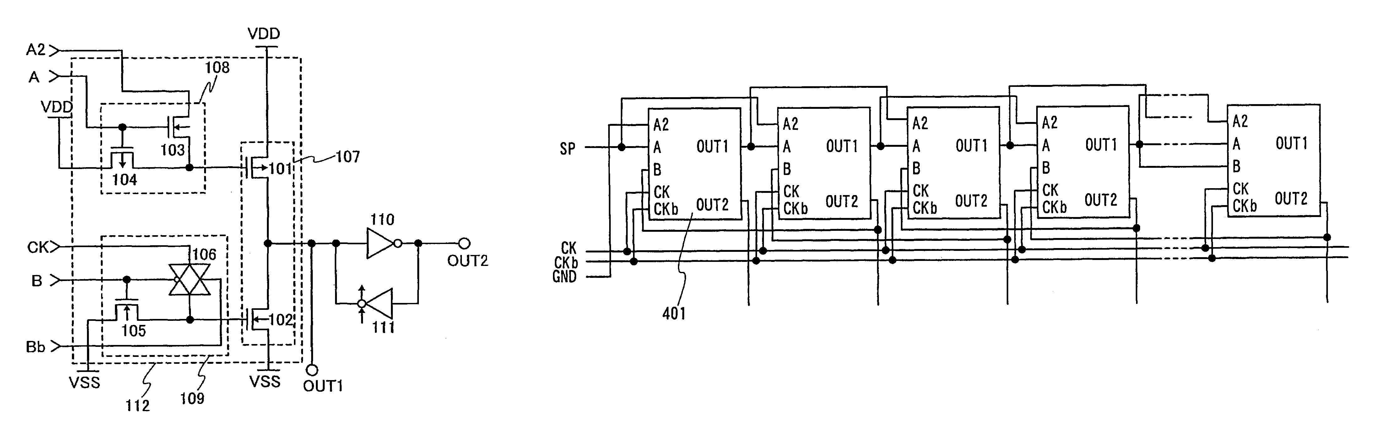
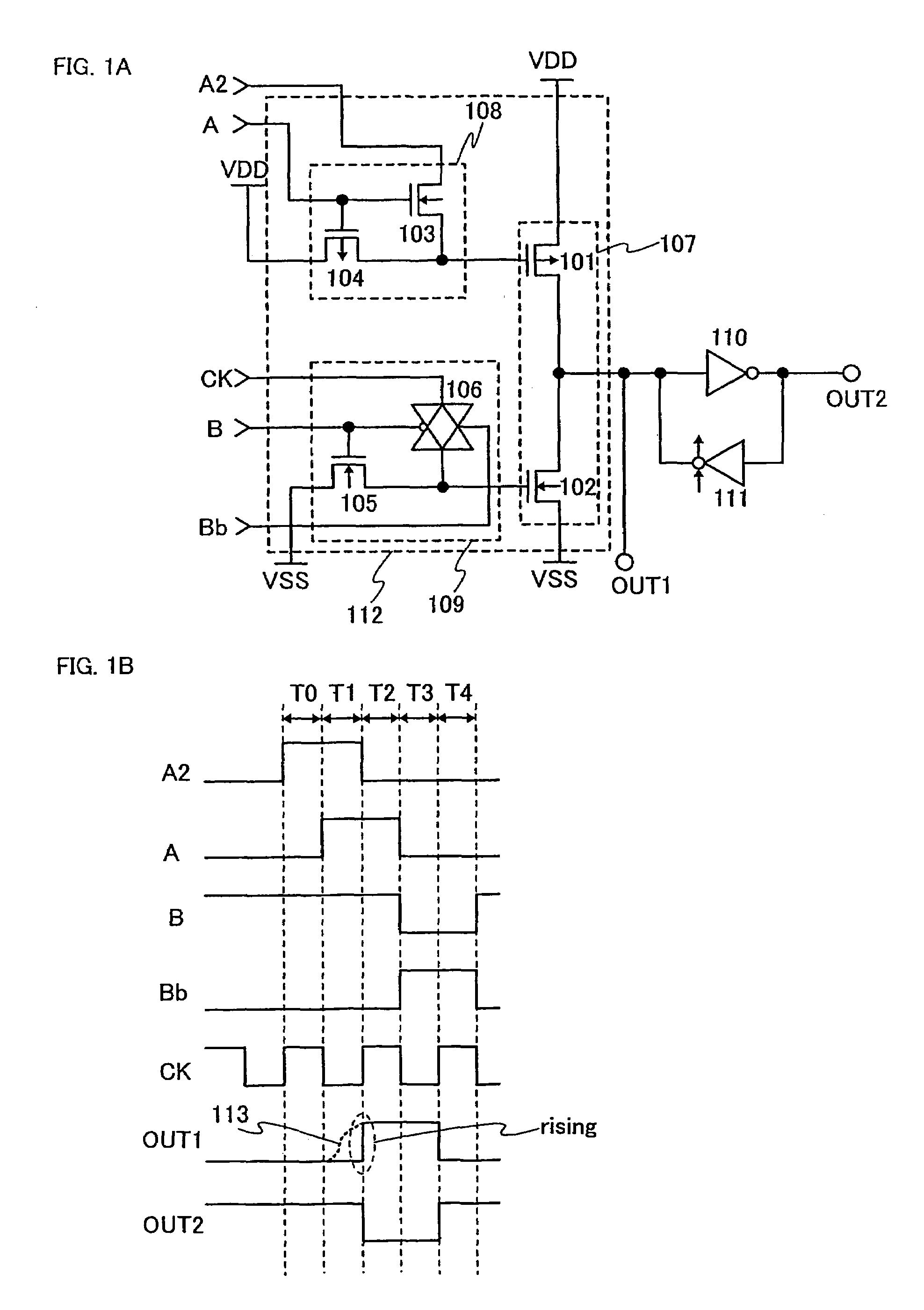
[0032]FIG. 1A shows one mode of a flip-flop circuit included in the shift register of the invention. The flip-flop circuit shown in FIG. 1A includes a clocked inverter 112, an inverter 110, and a clocked inverter 111. The clocked inverter 112 includes an inverter 107 including a transistor 101 and a transistor 102, a first compensation circuit 108 including a transistor 103 and a transistor 104, and a second compensation circuit 109 including a transistor 105 and a transmission gate 106.

[0033]The shift register of the invention includes a plurality of stages of flip-flop circuits which are inputted with clock signals alternately inverted per stage. For example, a terminal inputted with a clock signal CK in the preceding stage is inputted with an inverted clock signal CKb. On the contrary, a terminal inputted with an inverted clock signal CKb in the preceding stage is inputted with a clock signal CK.

[0034]In the inverter 107, each drain of the transistors 101 and 102 is connected to ...

embodiment mode 2

[0069]In this embodiment mode, a configuration of the shift register of the invention is described.

[0070]FIG. 3 shows a configuration of the shift register of this embodiment mode. The shift register of the invention includes a plurality of flip-flop circuits 401 each of which is inputted with the signal A from the output terminal OUT1 of the preceding stage, the signal A2 from the output terminal OUT1 of two stages before, and the signal B from the output terminal OUT2 of the succeeding stage. The flip-flop circuit 401 of the first stage is inputted with a start pulse signal SP instead of the signal A and supplied with a potential of ground instead of the signal A2. The flip-flop circuit 401 of the second stage is inputted with a start pulse signal SP instead of the signal A2. The flip-flop circuit 401 of the last stage is inputted with the signal A instead of the signal B.

[0071]A signal from the output terminal OUT2 of each of the flip-flop circuits 401 is inputted to the circuit ...

embodiment mode 3

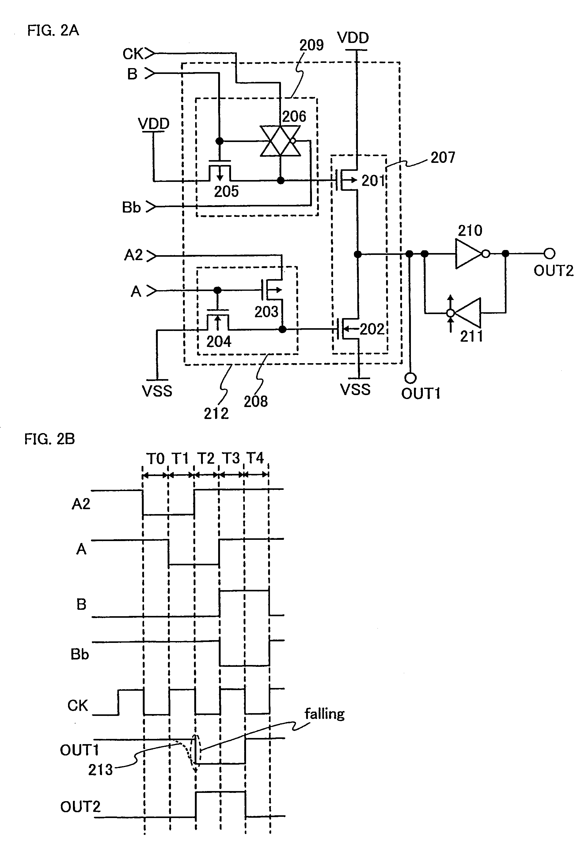
[0073]In this embodiment mode, a configuration for reducing a load imposed on a wiring for supplying the clock signal CK to a flip-flop circuit is described.

[0074]FIG. 4A shows an example in which an inverter 114 is used instead of the clocked inverter 111 in the flip-flop circuit shown in FIG. 1A. Note that in FIG. 4A, elements already shown in FIG. 1A are denoted by the same reference numerals.

[0075]In FIG. 4A, an output terminal of the inverter 110 and an input terminal of the inverter 114 are connected to the output terminal OUT2 of the flip-flop circuit. An input terminal of the inverter 110 and an output terminal of the inverter 114 are connected to the output terminal OUT1 of the clocked inverter 112.

[0076]In FIG. 4A, the number of the clocked inverters connected to a wiring for supplying the clock signal is less than that of the flip-flop circuit shown in FIG. 1A, thus a load imposed on the wiring can be reduced.

[0077]FIG. 4B shows an example in which an inverter 214 is used...


PUM

PropertyMeasurementUnit
diameteraaaaaaaaaa
threshold voltageaaaaaaaaaa

Abstract

The invention provides a shift register which can operate normally while suppressing a delay of signal and a rounding of waveform. The shift register of the invention includes a plurality of stages of flip-flop circuits each of which includes a clocked inverter. The clocked inverter includes a first transistor and a second transistor which are connected in series, a first compensation circuit including a third transistor and a fourth transistor which are connected in series, and a second compensation circuit including a fifth transistor and a transmission gate. According to the first compensation circuit, a timing at which a signal outputted from the flip-flop circuit rises or falls can be controlled in synchronization with an output of two stages before. The second compensation circuit can control a clock signal input can be controlled.

Description

TECHNICAL FIELD[0001]The present invention relates to a shift register. And also, the invention relates to a semiconductor display device including a shift register which is formed over the same substrate as a pixel portion.DESCRIPTION OF THE RELATED ARTBackground Art[0002]As the resolution becomes higher in an active matrix semiconductor display device formed by using an inexpensive glass substrate, a peripheral region (frame region) of a pixel portion used for mounting occupies larger area of the substrate, which prevents downsizing of the device. Therefore, there is a limit in a method for mounting an IC which is formed by using a single crystalline silicon wafer, thus a technique to form a driver circuit such as a signal line driver circuit and a scan line driver circuit over the same glass substrate as a pixel portion, that is a technique of System on Panel is considered important.[0003]A thin film transistor, however, has larger variations in characteristics such as a threshol...

Claims


Application Information

Patent Timeline
Patent Type & Authority Patents(United States)
IPC IPC(8): H03K23/00G02F1/133G09G3/20G09G3/32G09G3/36G11C19/00G11C19/28
CPCG09G3/3266G09G3/3275G11C19/28G09G3/3688G11C19/00G09G3/3677H03K19/018521
Inventor OSAME, MITSUAKIANZAI, AYA
Owner SEMICON ENERGY LAB CO LTD
Why Eureka
Try Eureka