Semiconductor device and method for manufacturing semiconductor device

Inactive Publication Date: 2005-04-21
KK TOSHIBA
View PDF2 Cites 21 Cited by
  • Summary
  • Abstract
  • Description
  • Claims
  • Application Information

AI Technical Summary

Benefits of technology

[0014] Therefore, the present invention solves the problems as described above, and provides a semiconductor device and a method for the manufacture thereof to avoid the depletion of the gate electrode even in the case where metals

Problems solved by technology

On the other hand, in gate electrodes, the lowering of capacitance due to depletion of the electrode causes problems with the miniaturization of transistors.
However, in general, for metal gates, methods equivalent to the method using polysilicon gate that can easily vary work functions by depositing a film, and then implanting each type of impurity to respective regions, have not been established.
However, the gate having a polysilicon film formed on the top has a high resistance of the electrode, and causes RC delay.
Therefore, the switching spee

Method used


Image

  • Semiconductor device and method for manufacturing semiconductor device
  • Semiconductor device and method for manufacturing semiconductor device
  • Semiconductor device and method for manufacturing semiconductor device

Examples


first embodiment

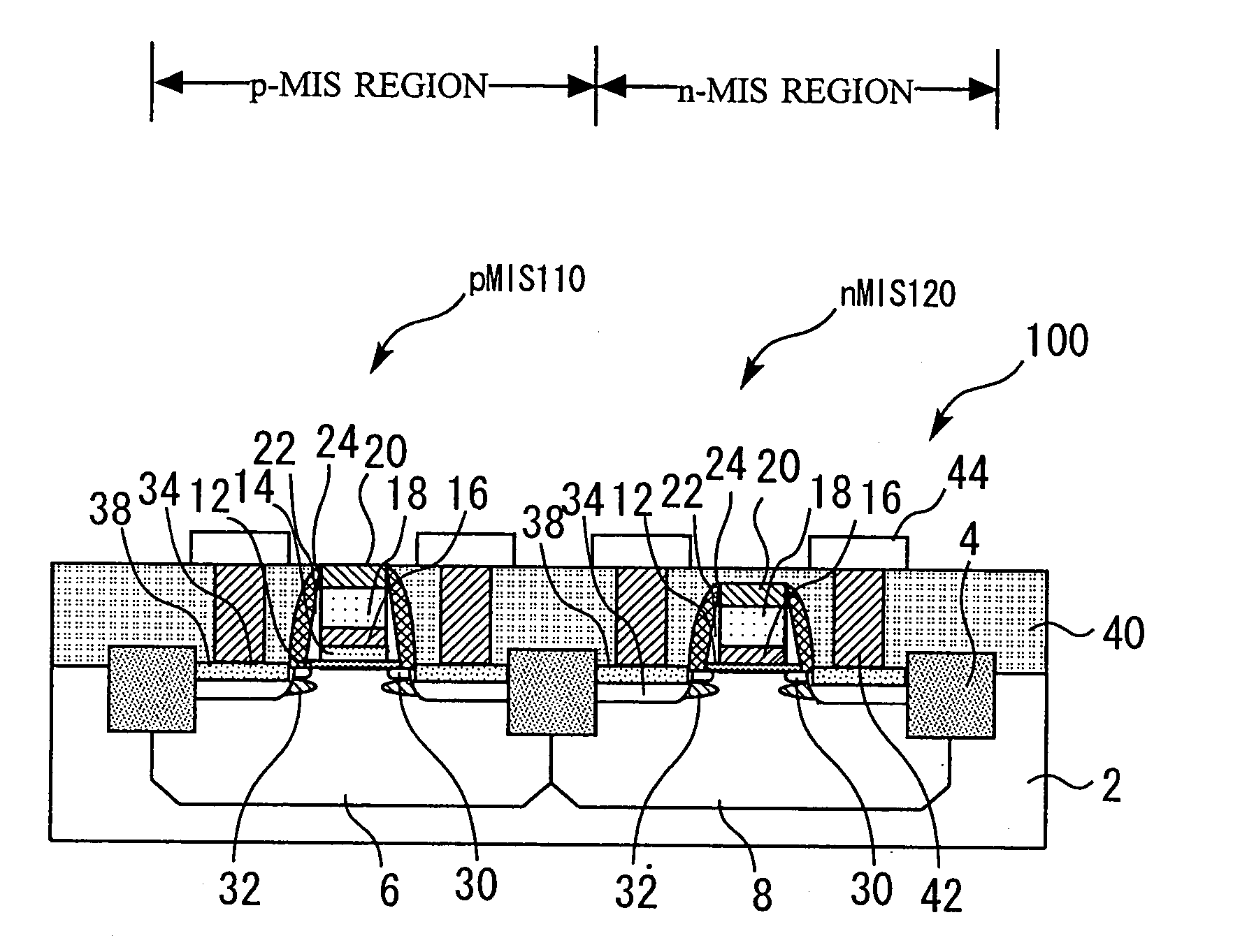
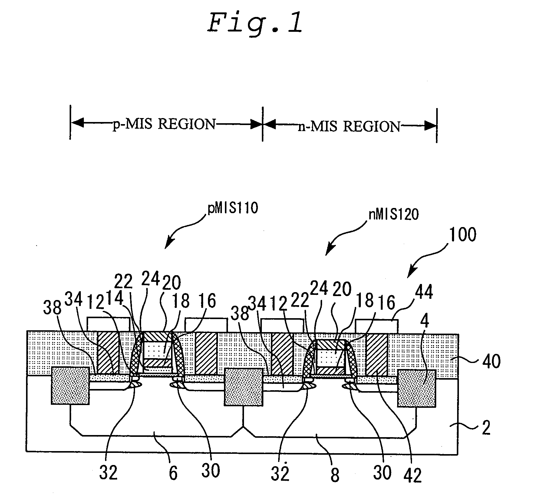
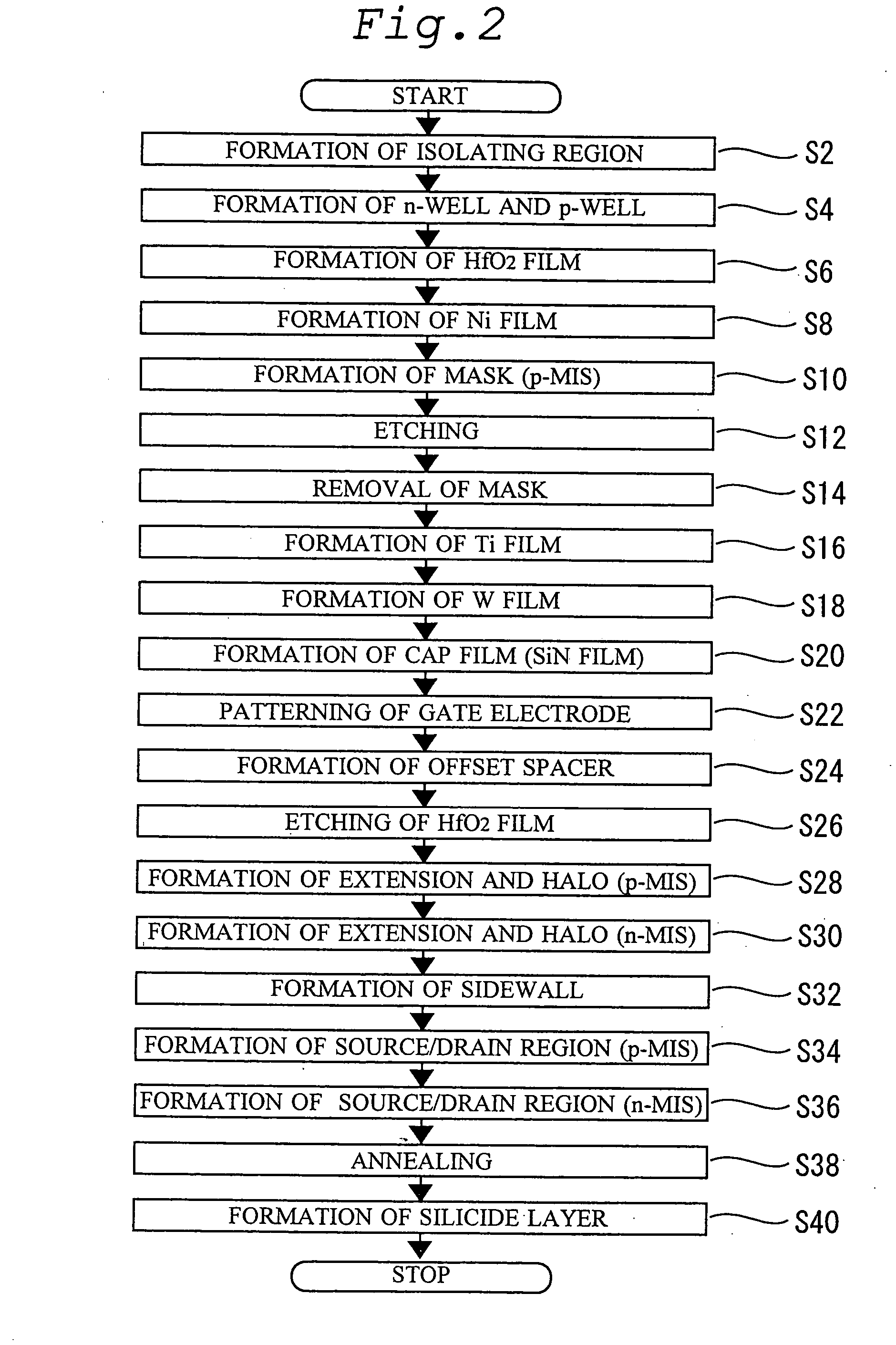
[0023]FIG. 1 is a schematic sectional view for illustrating a semiconductor device 100 according to the first embodiment of the present invention.

[0024] As FIG. 1 illustrates, a p-type MISFET (metal insulator semiconductor field effect transistor) 110 and an n-type MISFET 120 are formed in the semiconductor device 100. In this specification, the p-type MISFET 110 is referred to as the p-MIS 110, and the n-type MISFET 120 is referred to as the n-MIS 120 for simplifying description. The region for forming the p-MIS 110 and the region for forming the n-MIS 110 are referred to as the p-MIS region and the n-MIS region, respectively.

[0025] An isolating region 4 is formed on a silicon substrate 2, and the isolating region 4 divides the silicon substrate 2 into a p-MIS region and an n-MIS region. An n-well 6 and a p-well 8 are formed in the p-MIS region and the n-MIS region, respectively. In each region, an HfO2 film 12 is formed as a gate insulating film. The HfO2 film 12 is a high-diele...

second embodiment

[0075]FIG. 13 is a schematic sectional view for illustrating a semiconductor device according to the second embodiment of the present invention.

[0076] The semiconductor device 200 shown in FIG. 13 is similar to the semiconductor device 100 in the first embodiment.

[0077] However, in the semiconductor device 200, a laminated film composed of an SiO2 film 60 and an HfO2 film 62 is used in both the p-MIS 210 and the n-MIS 220, in place of the HfO2 film 12 used as the gate insulating film in the first embodiment.

[0078] In the p-MIS 210, a laminated film composed of a TiN film 64, a ZrN film 66, and a W film 68 is used as the gate electrode. In the n-MIS 220, a laminated film composed of a ZrN film 66 and a W film 68 is used as the gate electrode. In the same manner as the semiconductor device 100, a cap film 20 is formed on each gate electrode.

[0079] In also the second embodiment, an offset spacer 70 and a sidewall 72 are formed on the side of each gate electrode. The width of the wi...


PUM


Abstract

A gate insulating film is formed in a first region and a second region of a substrate, a first metallic film is formed on the gate insulating film in one of the first region or the second region, and a second metallic film is formed on each of the first and second regions. Furthermore, a protective film is formed on the second metallic film, and the protective film and the metallic film are patterned to the pattern of the gate electrode. Next, a first sidewall is formed on the side of a gate electrode. Then, impurities producing first and second conductivity types are implanted into the surface of the substrate in respective regions, using the first sidewalls and the gate electrodes as masks to form a first impurity-diffused region, and impurities producing second and first conductivity types are implanted to form an impurity diffusion preventing layer. Thereafter, a second sidewall is formed on the side of the first sidewall, and an impurity is implanted into the surface of the substrate using the second sidewalls and the gate electrodes as masks to form a second impurity-diffused region.

Description

BACKGROUND OF THE INVENTION [0001] 1. Field of the Invention [0002] The present invention relates to a semiconductor device and a method for manufacturing a semiconductor device. More specifically, the present invention relates to a semiconductor device including field-effect transistors, and a method for manufacturing such a semiconductor device. [0003] 2. Background Art [0004] In recent years, with the high integration and miniaturization of semiconductor devices, transistors have also been rapidly miniaturized. Concurrent therewith, the thickness of gate insulating films of transistors has been reduced to an EOT (equivalent oxide thickness) of about 2.0 nm or less. When the thickness of gate insulating films is so reduced, the leakage current of the conventional gate insulating films composed of SiO2 increases to the value not negligible. Therefore, a high-dielectric-constant film (hereafter abbreviated as high-k film) is used as the gate insulating film. When a high-k film is us...

Claims


Application Information

Patent Timeline
IPC IPC(8): H01L21/8238H01L29/76
CPCH01L21/823842
Inventor AKASAKA, YASUSHI
Owner KK TOSHIBA
Why Eureka
Try Eureka