NAND flash memory

a technology of flash memory and nand flash, which is applied in the field of nand flash, can solve the problems of requiring a very complicated fabrication process and it is not practicable to increase the memory density of conventional 3-dimensional memory designs by decreasing so as to achieve the effect of increasing the memory density, reducing the thickness of the ono stack, and simple fabrication process

Active Publication Date: 2013-10-31
DESIGN EXPRESS
View PDF3 Cites 5 Cited by
  • Summary
  • Abstract
  • Description
  • Claims
  • Application Information

AI Technical Summary

Benefits of technology

[0004]One aspect of the present disclosure provides a NAND flash memory structure capable of being vertically stacked to increase the memory capacity.
[0006]The conventional 3-dimensional memory designs implement the charge-trapping structure by the ONO stack laterally, requiring a very complicated fabrication process. In contrast, in one embodiment of the present disclosure, the charge-trapping structure is vertically aligned, allowing a relatively simple fabrication process.

Problems solved by technology

The conventional 3-dimensional memory designs implement the charge-trapping structure by the ONO stack laterally, requiring a very complicated fabrication process.
The thickness of the ONO stack serving as the charge-trapping structure is not a scalable parameter, and the it is not feasible to increase the memory density of the conventional 3-dimensional memory designs by decreasing the thickness of the ONO stack.

Method used


Image

  • NAND flash memory
  • NAND flash memory
  • NAND flash memory

Examples


Embodiment Construction

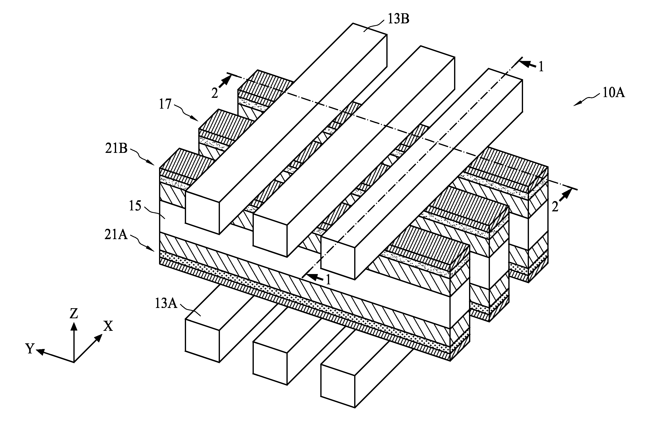
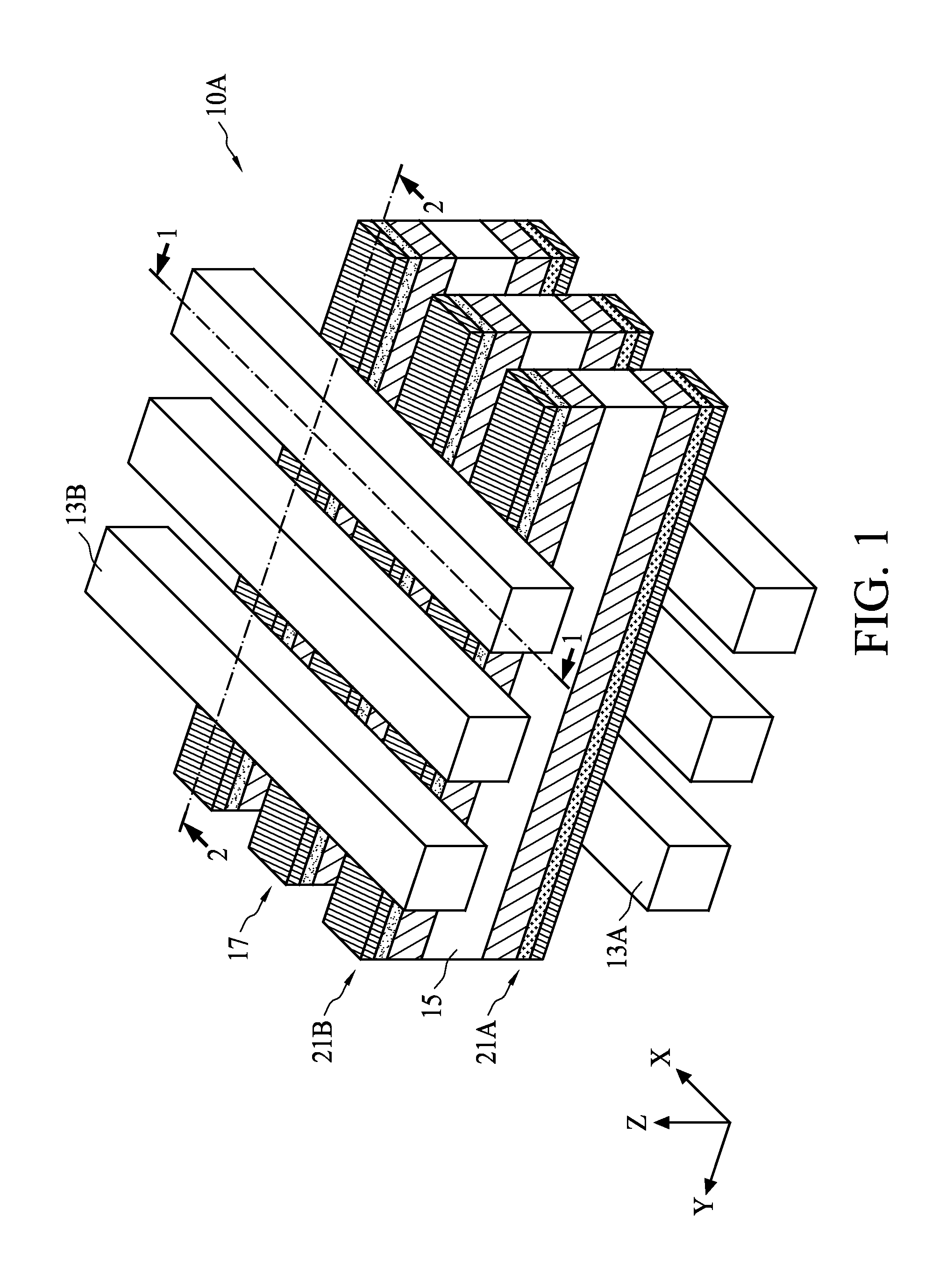
[0042]FIG. 1 illustrates a full view of a NAND flash memory structure 10A according to one embodiment of the present disclosure. For clearance purposes, the isolation material is omitted in FIG. 1. In one embodiment of the present invention, the NAND flash memory structure 10A comprises a plurality of first bitlines 13A, a plurality of second bitlines 13B, and a plurality of separated lines 17 between the first bitlines 13A and the second bitlines 13B. In one embodiment of the present invention, both the first bitlines 13A and the second bitlines 13B extend along a first direction substantially in a horizontal manner, and the separated lines 17 extend along a second direction substantially in a horizontal manner. In one embodiment of the present invention, the separated line 17 comprises a first charge-trapping stack 21A, a second charge-trapping stack 21B, and a wordline 15 positioned between the first charge-trapping stack 21A and the second charge-trapping stack 21B.
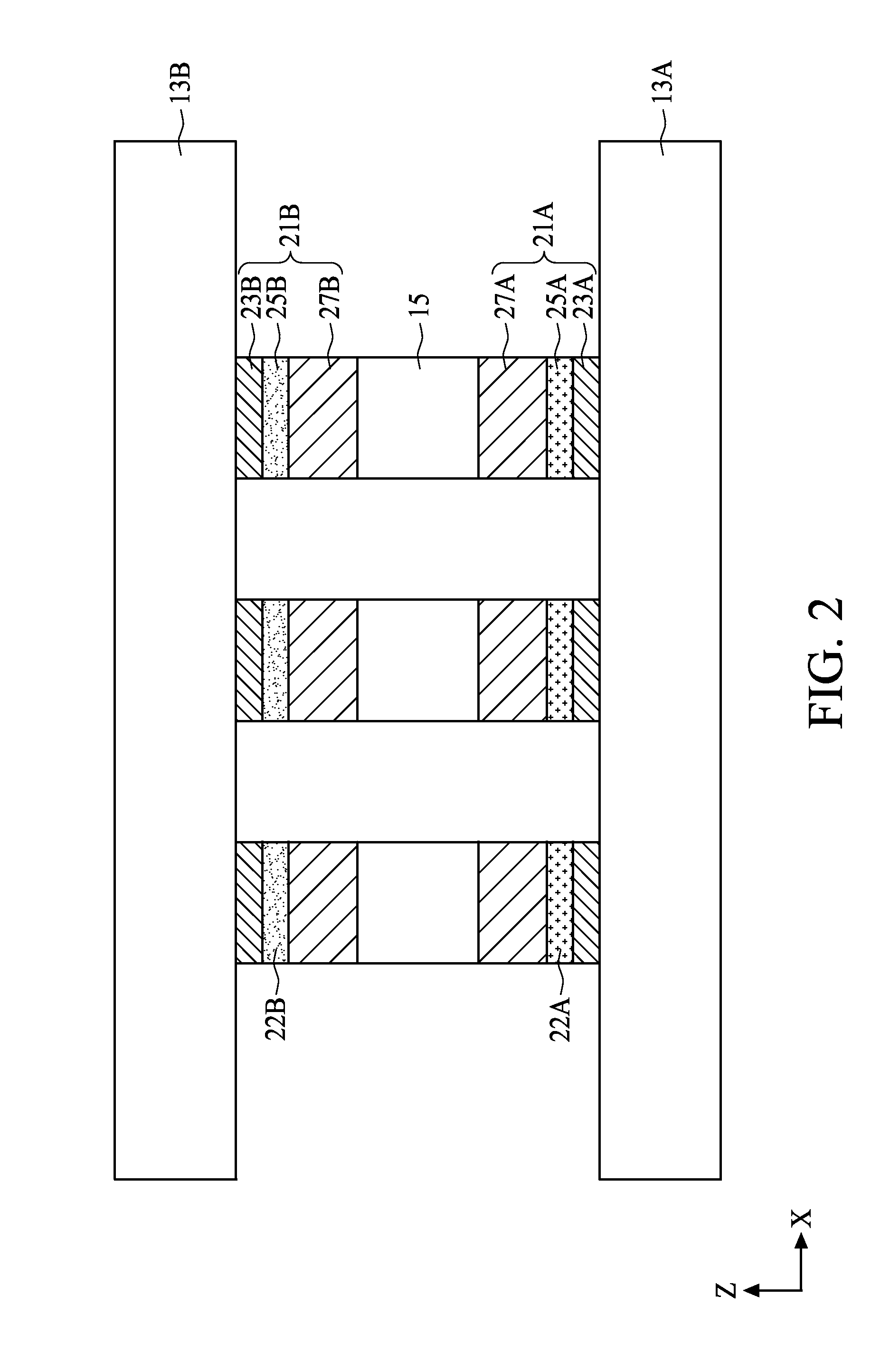
[0043]FIG. 2 ...


PUM


Abstract

A NAND flash memory includes a plurality of NAND flash memory structures separated by an insulating layer. In one embodiment of the present disclosure, the NAND flash memory structure includes a first bitline extending along a first direction, a first charge-trapping region positioned over the first bitline, a wordline positioned over the first charge-trapping region and extending along a second direction, a second charge-trapping region positioned over the wordline, and a second bitline positioned over the second charge-trapping region, wherein the first charge-trapping region and the second charge-trapping region are stacked along a third direction substantially perpendicular to the first direction and the second direction.

Description

TECHNICAL FIELD[0001]The present disclosure relates to a NAND flash, and more particularly, to a NAND flash memory capable of being vertically stacked to increase the memory capacity.BACKGROUND ART[0002]Flash memory has been widely applied to the data storage of digital products such as laptop computers, personal digital assistants, cellular telephones, digital cameras, digital recorders, and MP3 players. In order to keep up with customer demand for low-priced, efficient, small devices with high capacity, there is a growing need for highly integrated semiconductor memories. Accordingly, the use of 3-dimensional designs has been proposed for semiconductor memories. For example, conventional 3-dimensional memory designs such as Pipe-shaped Bit Cost Scalable (P-BiCS), Vertical Cell Array using TCAT (Terabit Cell Array Transistor), Vertical-Stacked-Array-Transistor (VSAT), and Vertical Gate NAND (VG-NAND) have been proposed to meet the growing need for highly integrated semiconductor me...

Claims


Application Information

Patent Timeline
Patent Type & Authority Applications(United States)
IPC IPC(8): G11C16/04
CPCG11C16/0466H01L29/792H01L29/66833H10B43/10H10B43/23H10B43/20
Inventor CHANG, CHUN-YEN
Owner DESIGN EXPRESS
Why Eureka
Try Eureka