
Signal source synchronization circuit

a synchronization circuit and signal source technology, applied in the direction of synchronization receivers, digital transmission, generating/distributing signals, etc., can solve the problem of degrading the accuracy of synchronization

Active Publication Date: 2013-10-31
MITSUBISHI ELECTRIC CORP
View PDF1 Cites 14 Cited by
  • Summary
  • Abstract
  • Description
  • Claims
  • Application Information

AI Technical Summary

Benefits of technology

The present invention provides a signal source synchronization circuit that can improve the accuracy of synchronization among individual signal source circuits. The circuit uses two time difference measurement circuits to determine the time difference between the input time of a trigger signal and the input time of the trigger signal from a different signal source circuit. The first signal source circuit adjusts the phase of the reference signal based on the time difference measured by the first circuit, while the second signal source circuit adjusts the phase of the reference signal based on the time difference measured by the second circuit. This results in a more accurate synchronization between the signal source circuits.

Problems solved by technology

As a result, there is a problem such that variations in signal timing occur in the signal source circuits and accuracy in synchronization is degraded.

Method used


Image

  • Signal source synchronization circuit
  • Signal source synchronization circuit
  • Signal source synchronization circuit

Examples


embodiment 1

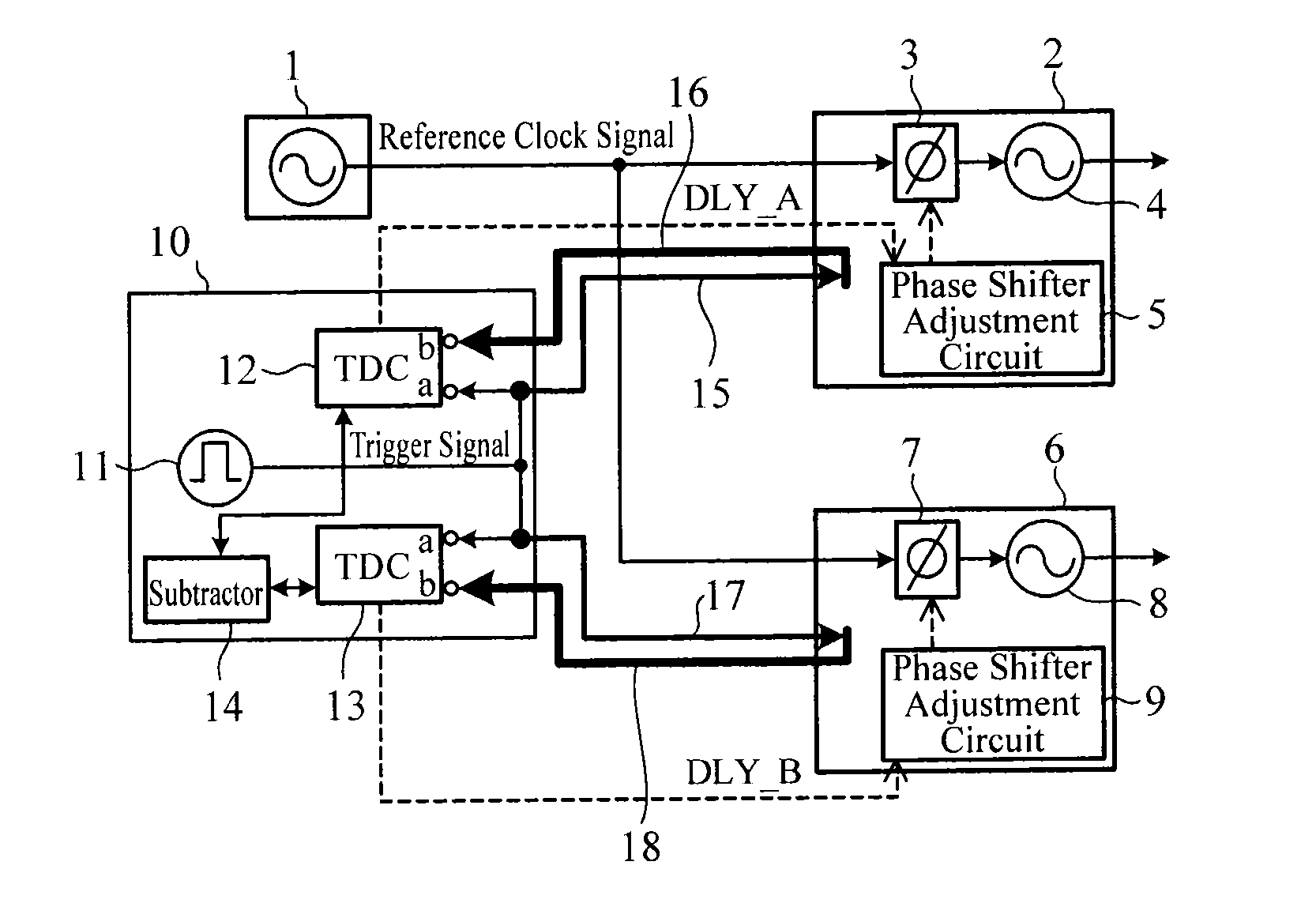
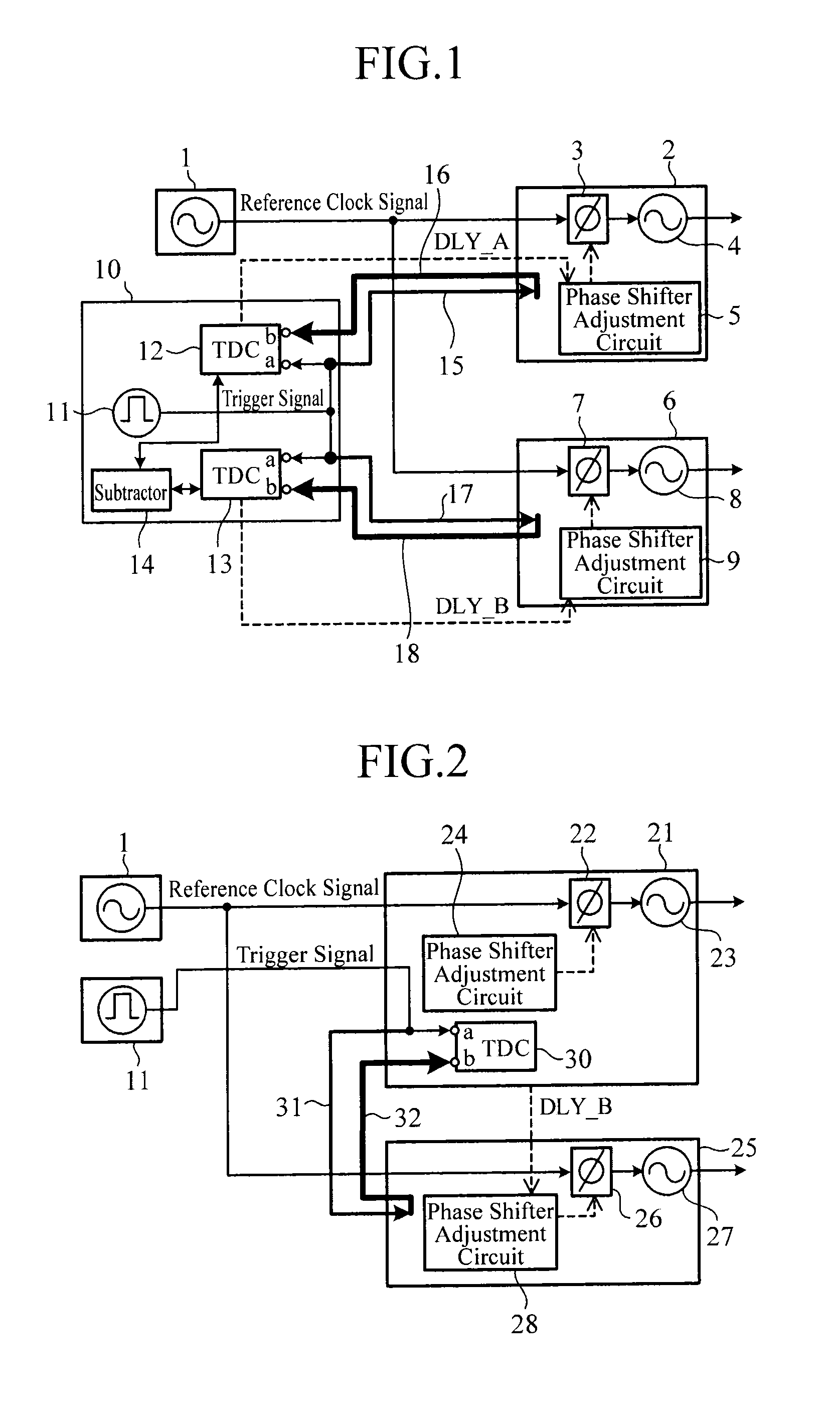
[0017]FIG. 1 is a block diagram showing a signal source synchronization circuit according to Embodiment 1 of the invention.

[0018]In FIG. 1, a reference signal source 1 is a signal source that generates a reference clock signal (reference signal).

[0019]A signal source circuit 2 is constituted by a phase shifter 3, a local oscillator 4, and a phase shifter adjustment circuit 5, adjusts the phase of the reference clock signal generated by the reference signal source 1, and generates a signal synchronized with the reference clock signal after the phase adjustment. Note that the signal source circuit 2 constitutes a first signal source circuit.

[0020]The phase shifter 3 of the signal source circuit 2 adjusts the phase of the reference clock signal generated by the reference signal source 1 by a phase adjustment amount set by the phase shifter adjustment circuit 5.

[0021]The local oscillator 4 generates a signal synchronized with the reference clock signal having the phase adjusted by the p...

embodiment 2

[0069]Although Embodiment 1 described above has shown an example in which the trigger signal outputted from the trigger signal generation circuit 11 is inputted to each of the signal source circuits 2 and 6 and then fed back, in a case where the distance from the trigger signal generation circuit 11 to each of the signal source circuits 2 and 6 is long, path lengths of the signal paths 15 and 17 and the feedback paths 16 and 18 to the signal source circuits 2 and 6 are increased, respectively. As a result, it is necessary to prepare cables having a long path length corresponding to the number of the signal source circuits.

[0070]In Embodiment 2, the number of the cables having a long path length is reduced in the following manner.

[0071]FIG. 2 is a block diagram showing a signal source synchronization circuit according to Embodiment 2 of the invention. In the drawing, the same reference numerals as those in FIG. 1 denote the same or equivalent portions, and hence descriptions thereof ...

embodiment 3

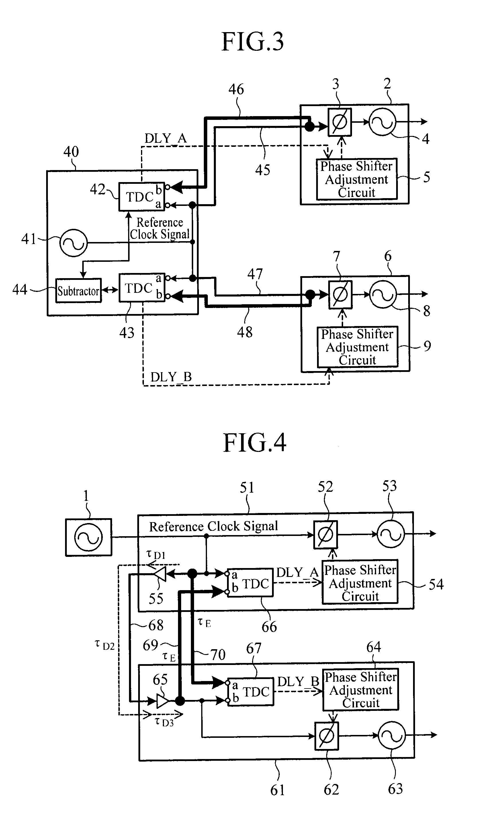
[0104]Although Embodiment 1 described above has shown an example in which the trigger signal generation circuit 11 is implemented in addition to the reference signal source 1, the phases of the signal generated by the signal source circuit 2 and the signal generated by the signal source circuit 6 may be caused to coincide with each other by using the reference clock signal without implementing the trigger signal generation circuit 11.

[0105]In a case where the phase difference between the signal generated by the signal source circuit 2 and the signal generated by the signal source circuit 6 is sufficiently small relative to the cycle of the reference clock signal, it is possible to detect the phase difference by comparing the rising edge timings of the reference clock signals.

[0106]FIG. 3 is a block diagram showing a signal source synchronization circuit according to Embodiment 3 of the invention. In the drawing, the same reference numerals as those in FIG. 1 denote the same or equiv...


PUM


Abstract

A signal source synchronization circuit includes: a first TDC circuit that measures a first path delay time which is a time difference between an input time of a trigger signal to a first input terminal and an input time of the trigger signal to a second input terminal; and a second TDC circuit that measures a second path delay time which is a time difference between an input time of the trigger signal to a first input terminal and an input time of the trigger signal to a second input terminal, wherein a first phase shifter adjustment circuit sets a phase adjustment amount corresponding to the first path delay time in a first phase shifter, and a second phase shifter adjustment circuit sets a phase adjustment amount corresponding to the second path delay time in a second phase shifter.

Description

BACKGROUND OF THE INVENTION[0001]1. Field of the Invention[0002]The present invention relates to a signal source synchronization circuit that achieves synchronization of frequencies and phases among a plurality of signal source circuits.[0003]2. Description of Related Art[0004]For example, in a signal source synchronization circuit disclosed in MIMO NOTAMENO TASHINGOGEN NO DOUKIKA (Multiple Source Synchronization for MIMO), Application Note, Anritsu, September 2007, synchronization of frequencies is achieved by inputting a signal of 10 MHz outputted from a reference signal source to two measuring instruments, and synchronization of phases of two measuring instruments is achieved by a trigger signal outputted from a trigger generator.[0005]Since the conventional signal source synchronization circuit is structured as mentioned above, in a case where distances between the signal source circuits and the trigger generator are not the same, an arrival time of the trigger signal differs de...

Claims


Application Information

Patent Timeline
IPC IPC(8): H04L7/00
CPCH04L7/0079G06F1/10G06F1/12
Inventor NAKAMIZO, HIDEYUKITAJIMA, KENICHIANDO, NOBUHIKOKAWAKAMI, KENJI
Owner MITSUBISHI ELECTRIC CORP
Learn More