

Fabrication method of trench power semiconductor structure
- Summary
- Abstract
- Description
- Claims
- Application Information
AI Technical Summary
Benefits of technology
Problems solved by technology
Method used
Image

Examples
Embodiment Construction
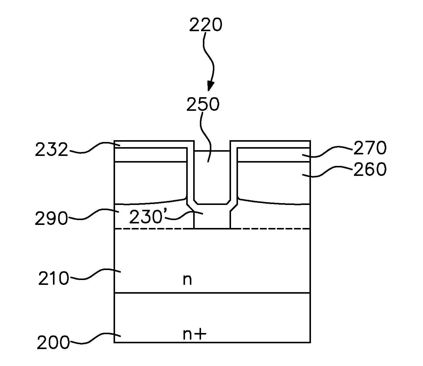
[0016]The technological feature of the present invention is to form a dielectric layer having a predetermine thickness on a first epitaxial layer. Since the growth speed of the dielectric layer is easy to be controlled, desired thickness of the dielectric layer may be exactly formed on the first epitaxial layer. As the predetermine thickness of the dielectric layer can be formed on the first epitaxial layer, a shielding layer can then be formed on the dielectric layer. Consequently, the step of etching dielectric layer may be prevented in the present invention. The exact value and even thickness of the dielectric layer may be achieved in the bottom of the gate trench. Therefore, the damage of the dielectric layer due to etching step may be avoided.
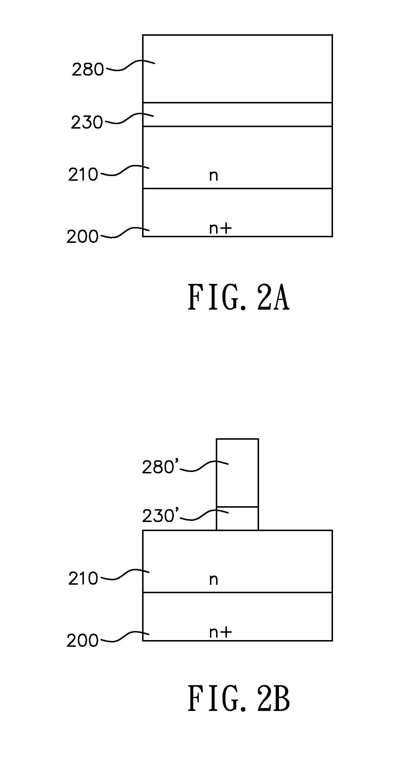
[0017]FIG. 2A to FIG. 2E schematically illustrates a fabrication method of a trench power semiconductor structure according to a first embodiment of the present invention. Firstly, referring to FIG. 2A, a heavily doped N-type substrate 200...
PUM
 Abstract
Description
Claims
Application Information