

Substrate cleaning apparatus
a cleaning apparatus and substrate technology, applied in the direction of cleaning process and apparatus, chemistry apparatus and processes, cleaning using liquids, etc., can solve the problems that the conventional substrate cleaning apparatus cannot meet the requirements for cleaning an entire surface of the substrate uniformly, and achieve the effect of uniform cleaning and efficient cleaning
- Summary
- Abstract
- Description
- Claims
- Application Information
AI Technical Summary
Benefits of technology
Problems solved by technology
Method used
Image

Examples
Embodiment Construction
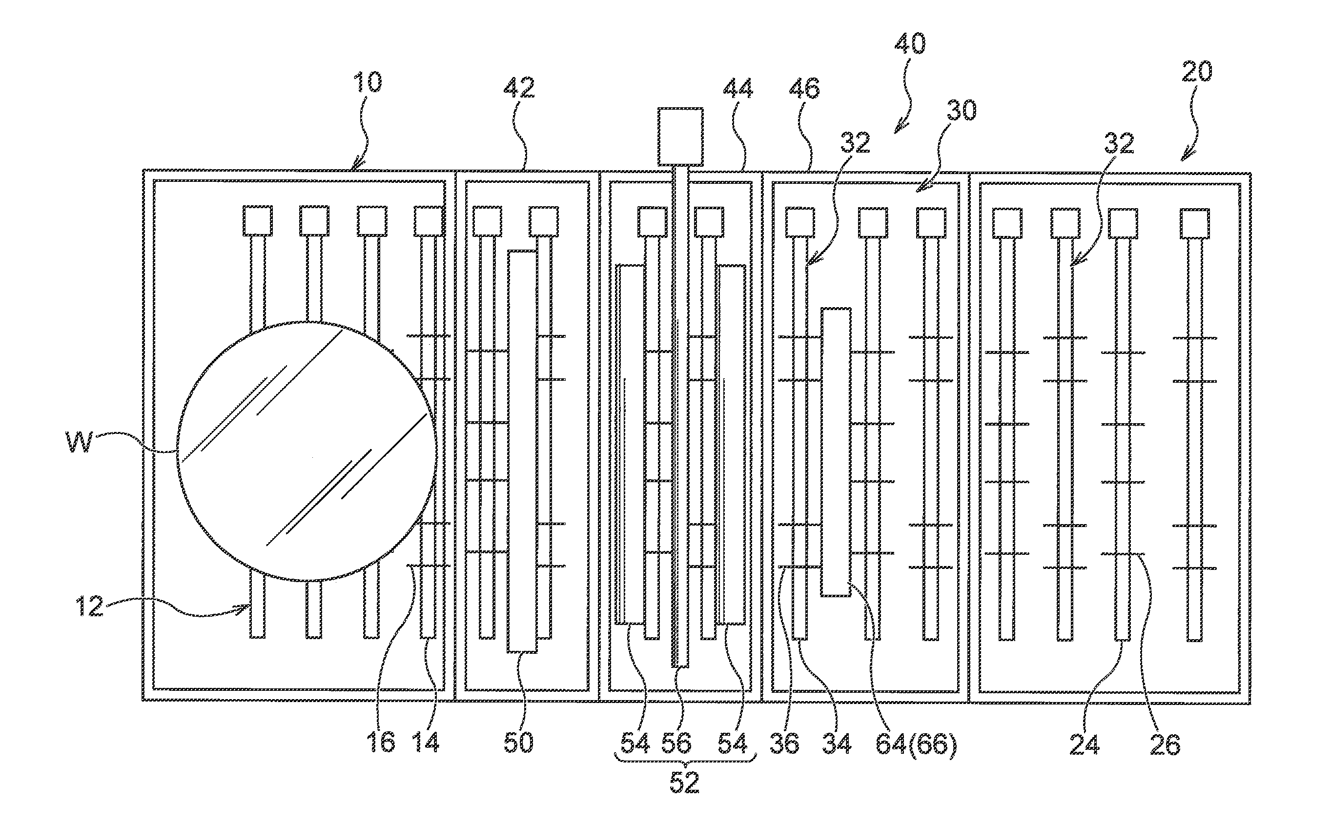
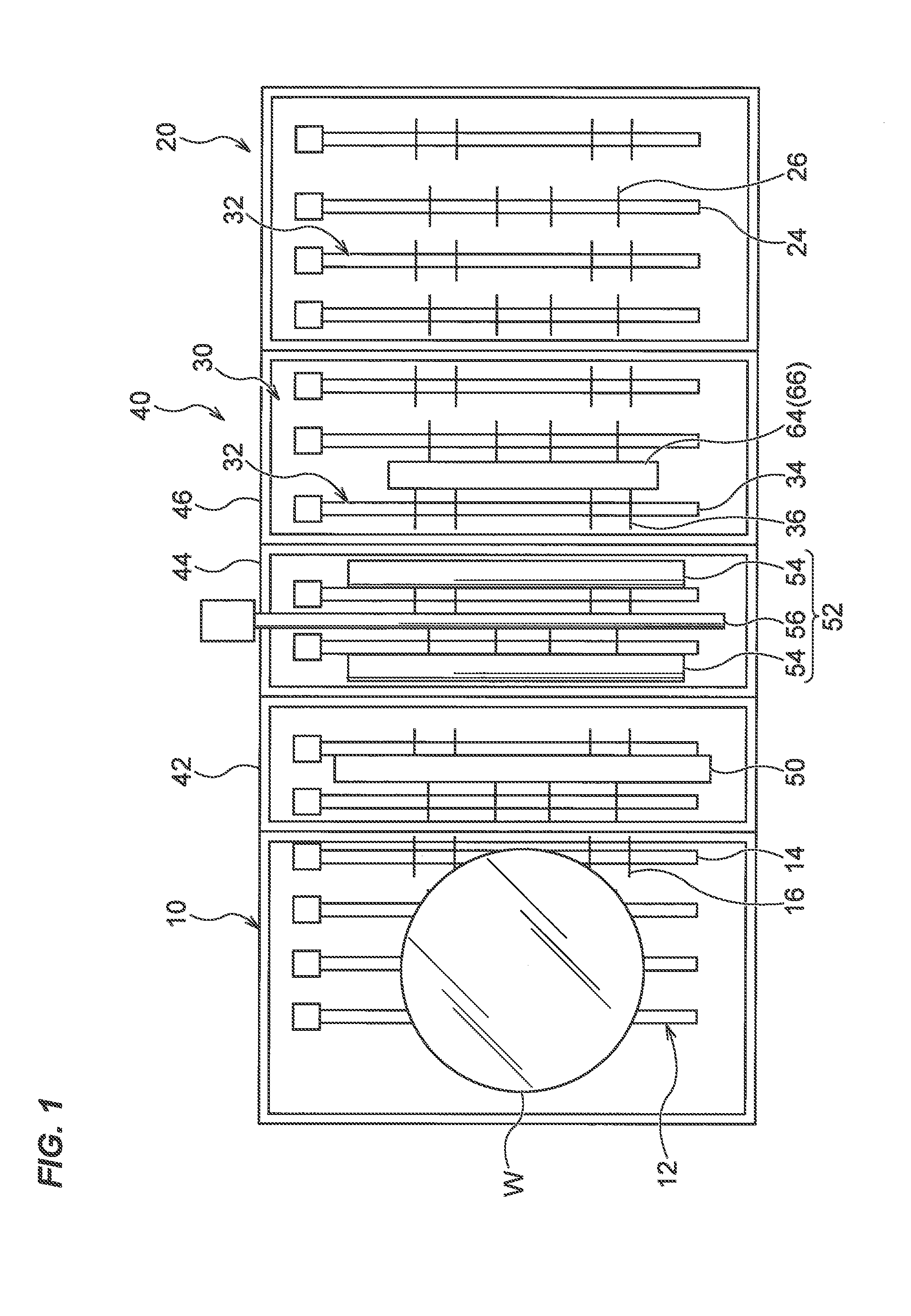
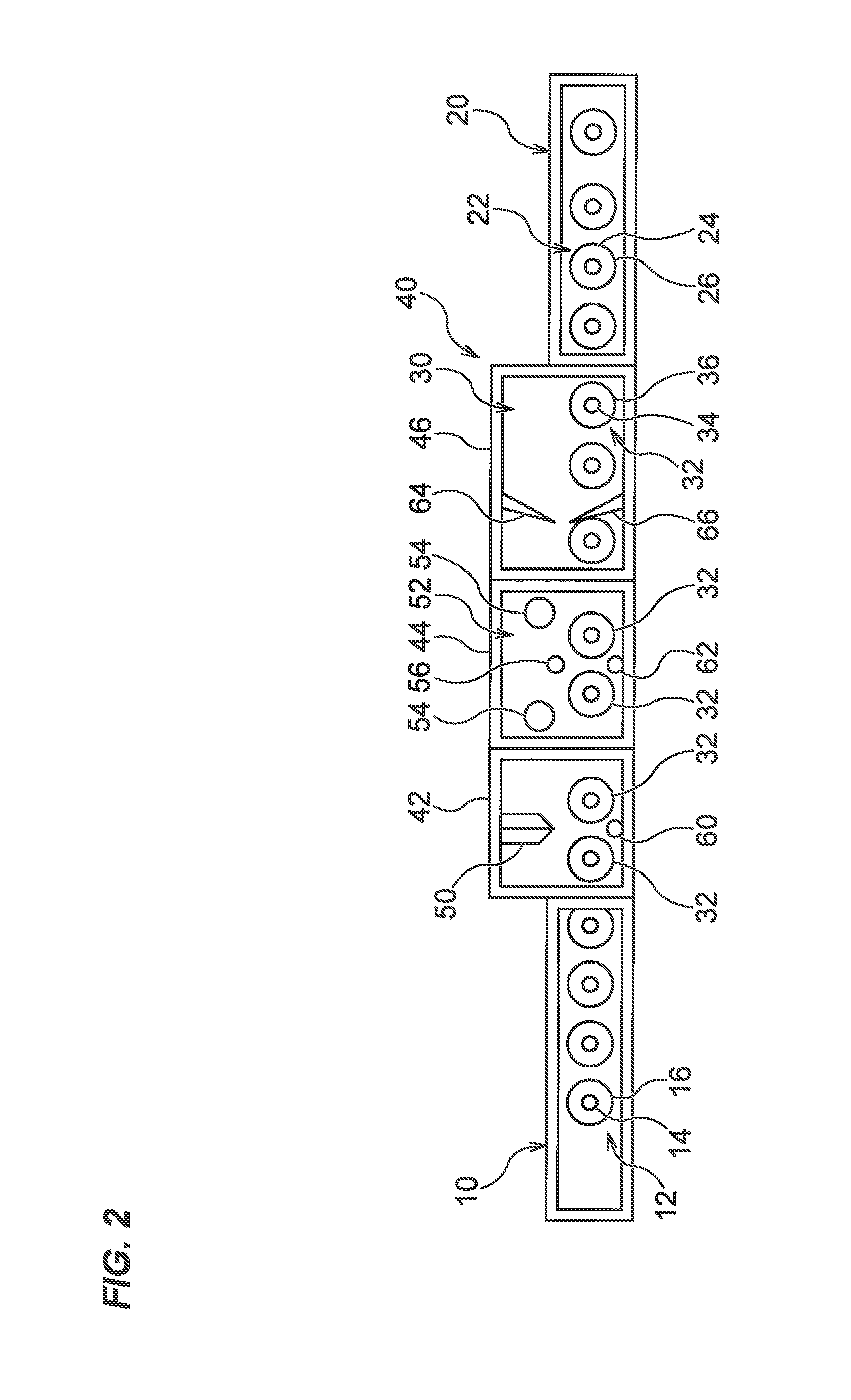
[0038]A substrate cleaning apparatus according to embodiments of the present invention will be described below with reference to FIGS. 1 to 6. Identical or corresponding parts are denoted by identical reference numerals in FIGS. 1 to 6, and will not be described in duplication.
[0039]FIG. 1 is a plan view showing a substrate cleaning apparatus according to an embodiment of the present invention. FIG. 2 is a sectional elevational view of the substrate cleaning apparatus shown in FIG. 1. As shown in FIGS. 1 and 2, the substrate cleaning apparatus comprises an inlet roller conveyer 10 and an outlet roller conveyer 20, and a process chamber 40 disposed between the inlet roller conveyer 10 and the outlet roller conveyer 20 and having an inner roller conveyer 30 serving as a substrate conveying unit therein. These roller conveyers 10, 20 and 30 are configured to convey substrates horizontally in a sliding manner, with their front surfaces facing upwardly.
[0040]The inlet roller conveyer 10 ...
PUM
 Abstract
Description
Claims
Application Information