Transistor structure and driving circuit structure

a technology of transistors and circuits, applied in the direction of semiconductor devices, instruments, electrical devices, etc., can solve the problems of deteriorating the stability and reliability of tft, and achieve the effect of favorable stability and reliability

Active Publication Date: 2013-11-21
AU OPTRONICS CORP
View PDF6 Cites 4 Cited by
  • Summary
  • Abstract
  • Description
  • Claims
  • Application Information

AI Technical Summary

Benefits of technology

[0008]The invention is directed to a transistor structure featuring favorable stability and reliability.

Problems solved by technology

Nonetheless, when the channel width is increased, and the channel length is decreased, the notable self-heating effect of the TFT may deteriorate the stability and reliability of the TFT.

Method used


Image

  • Transistor structure and driving circuit structure
  • Transistor structure and driving circuit structure
  • Transistor structure and driving circuit structure

Examples


Embodiment Construction

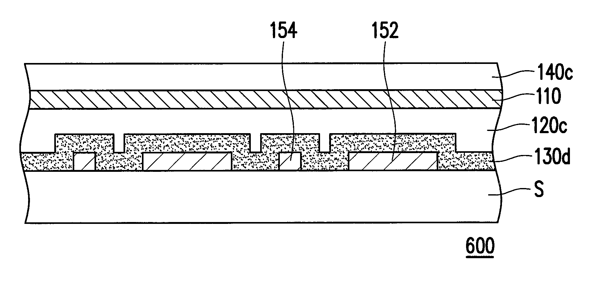
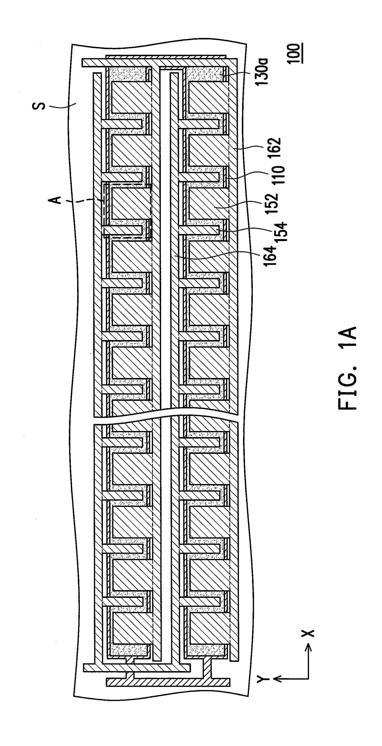
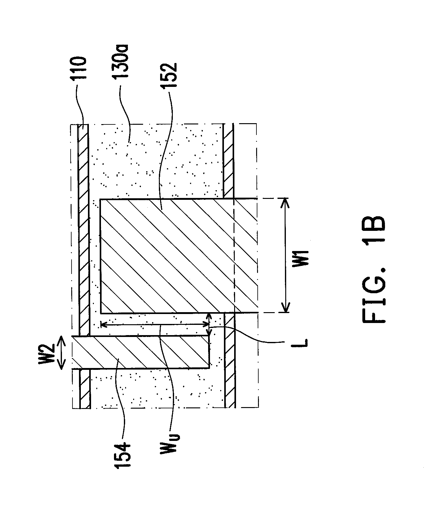
[0039]FIG. 1A is a schematic top view illustrating a transistor structure according to an embodiment of the invention. FIG. 1B is an enlarged view schematically illustrating an area A depicted in FIG. 1A. With reference to FIG. 1A and FIG. 1B, the transistor structure 100 described in this embodiment is disposed on a substrate S, and the substrate S may be made of glass, alkali glass, quartz, polyester, polycarbonate, flexible plastic materials, other flexible materials, or any other appropriate material. Specifically, the transistor structure 100 includes a gate electrode 110, a channel layer 130a overlapping the gate electrode 110, and a plurality of first electrodes 152 and a plurality of second electrodes 154 overlapping the gate electrode 110.

[0040]The channel layer 130a may include a semiconductor layer. That is, the channel layer 130a may be a semiconductor layer having the single-layer structure or the multi-layer structure. In the present embodiment, the semiconductor layer...


PUM


Abstract

A transistor structure disposed on a substrate includes a gate electrode, a gate insulating layer overlapping the gate electrode, a channel layer overlapping the gate electrode, and a plurality of first electrodes and a plurality of second electrodes overlapping the gate electrode. The gate insulating layer is disposed between the channel layer and the gate electrode. Besides, the gate insulating layer is located among the first electrodes, the second electrodes, and the gate electrode. The first electrodes and the second electrodes are alternately arranged along a first direction. Each of the first electrodes has a first width along the first direction. Each of the second electrodes has a second width along the first direction. A ratio of the first width to the second width ranges from 2 to 20. A driving circuit structure having the transistor structure is also provided.

Description

CROSS-REFERENCE TO RELATED APPLICATION[0001]This application claims the priority benefit of Taiwan application serial no. 101117988, filed on May 21, 2012. The entirety of the above-mentioned patent application is hereby incorporated by reference herein and made a part of this specification.BACKGROUND OF THE INVENTION[0002]1. Field of the Invention[0003]The invention relates to a semiconductor device structure and a circuit structure. More particularly, the invention relates to a transistor structure and a driving circuit structure.[0004]2. Description of Related Art[0005]Among various flat panel displays, thin film transistor liquid crystal displays (TFT-LCD) characterized by great space utilization, low power consumption, non-radiation, and low electromagnetic interference gain popularity among consumers. The TFT-LCD is mainly constituted by an active array substrate, a color filter substrate, and a liquid crystal layer sandwiched between the two substrates. The active array subst...

Claims


Application Information

Patent Timeline
Patent Type & Authority Applications(United States)
IPC IPC(8): H01L29/786
CPCH01L29/41733H01L27/124G09G3/3674G09G2310/0286
Inventor CHANG, JYU-YULAI, CHUN-WEISHEN, PO-YUANLEE, WEN-JUNGTAI, CHIH-WEI
Owner AU OPTRONICS CORP
Why Eureka
Try Eureka