Hybrid intergrated component

Active Publication Date: 2013-11-21
ROBERT BOSCH GMBH
View PDF0 Cites 13 Cited by
  • Summary
  • Abstract
  • Description
  • Claims
  • Application Information

AI Technical Summary

Benefits of technology

[0016]The concept according to the present invention is suited in particular for implementing hybrid integrated sensor components which operate in a contactless manner, for example, inertial sensor components, since the sensor structure is enclosed hermetically between the MEMS substrate and the ASIC cap here, and is thus protected from soiling and an aggressive measuring environment. In the case of an inertial sensor component, the micromec

Problems solved by technology

Printed conductors in the printed conductor level of the MEMS element have a minimum wid

Method used


Image

  • Hybrid intergrated component
  • Hybrid intergrated component
  • Hybrid intergrated component

Examples


Embodiment Construction

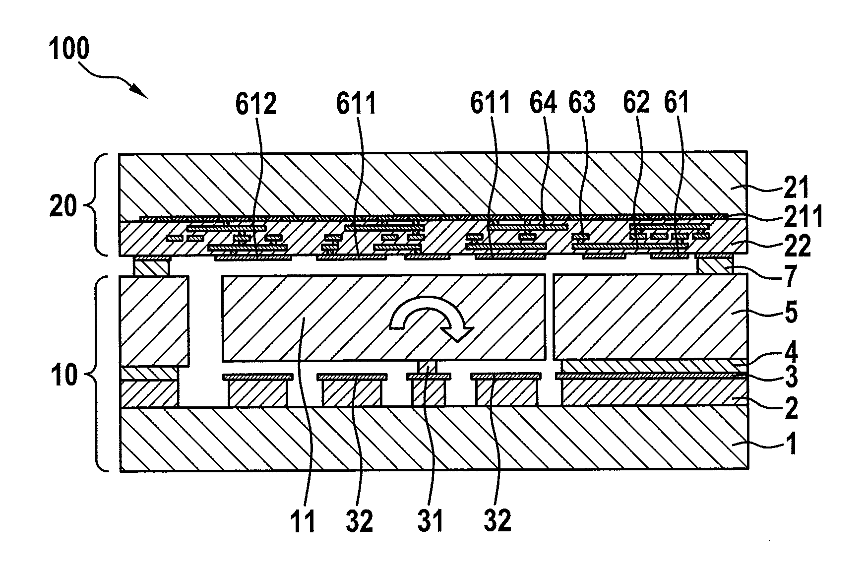
[0018]Sensor component 100 shown in FIGS. 1a and 1b essentially includes an MEMS element 10 and an ASIC element 20. The functionality of MEMS element 10 is implemented in a layered structure on a semiconductor substrate 1. This may be a silicon substrate, for example. The layered structure includes a printed conductor level 3 and a functional layer 5. Printed conductor layer 3 is implemented here in the form of a doped polysilicon layer, which was deposited on semiconductor substrate 1 above a first insulating layer 2 made of silicon oxide. Individual areas of printed conductor level 3 were spatially separated from one another by structuring of polysilicon layer 3, to thus produce printed conductors, a terminal area 31 for the micromechanical sensor structure, and also two stationary electrodes 32 of a measuring capacitor system. The two stationary electrodes 32 of the measuring capacitor system are situated symmetrically on both sides of terminal area 31. Another oxide layer 4 was ...


PUM


Abstract

A hybrid integrated component including an MEMS element and an ASIC element is refined to improve the capacitive signal detection or activation. The MEMS element is implemented in a layered structure on a semiconductor substrate. The layered structure of the MEMS element includes at least one printed conductor level and at least one functional layer, in which the micromechanical structure of the MEMS element having at least one deflectable structural element is implemented. The ASIC element is mounted face down on the layered structure and functions as a cap for the micromechanical structure. The deflectable structural element of the MEMS element is equipped with at least one electrode of a capacitor system. At least one stationary counter electrode of the capacitor system is implemented in the printed conductor level of the MEMS element, and the ASIC element includes at least one further counter electrode of the capacitor system.

Description

FIELD OF THE INVENTION[0001]The present invention relates to a component including at least one MEMS (micro-electromechanical system) element and at least one ASIC (application specific integrated circuit) element. The functionality of the MEMS element is implemented in a layered structure on a semiconductor substrate. This layered structure includes at least one printed conductor level and at least one functional layer, in which the micromechanical structure of the MEMS element having at least one deflectable structural element is implemented. The printed conductor level is, on the one hand, insulated by at least one insulating layer from the semiconductor substrate and, on the other hand, insulated by at least one insulating layer from the functional layer. The ASIC element is mounted face down on the layered structure of the MEMS element and functions as a cap for the micromechanical structure of the MEMS element.[0002]The MEMS element may be a sensor element having a circuit for...

Claims


Application Information

Patent Timeline
IPC IPC(8): B81B7/00
CPCB81B7/008B81C1/0023B81C1/00238B81C2203/0792
Inventor CLASSEN, JOHANNESFREY, JENS
Owner ROBERT BOSCH GMBH
Why Eureka
Try Eureka