

Methods for fabricating finfet integrated circuits on bulk semiconductor substrates
a technology of integrated circuits and semiconductor substrates, applied in the direction of basic electric elements, electrical apparatus, semiconductor devices, etc., can solve the problems of affecting the processing efficiency of the integrated circuit, the inability to meet the requirements of the substrate,
- Summary
- Abstract
- Description
- Claims
- Application Information
AI Technical Summary
Benefits of technology
Problems solved by technology
Method used
Image

Examples
Embodiment Construction
[0011]The following detailed description is merely exemplary in nature and is not intended to limit the invention or the application and uses of the invention. Furthermore, there is no intention to be bound by any expressed or implied theory presented in the preceding technical field, background, brief summary or the following detailed description.
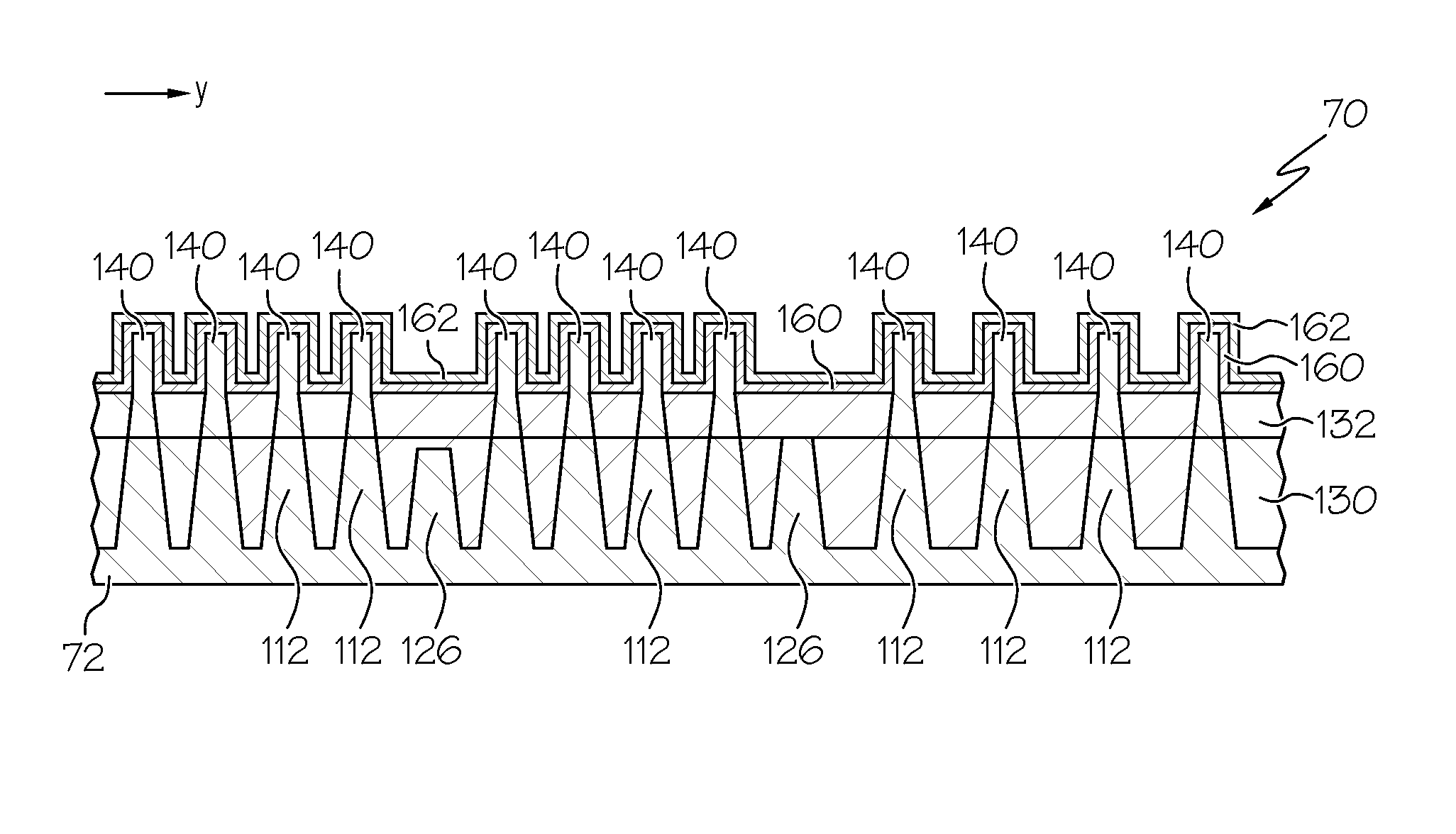
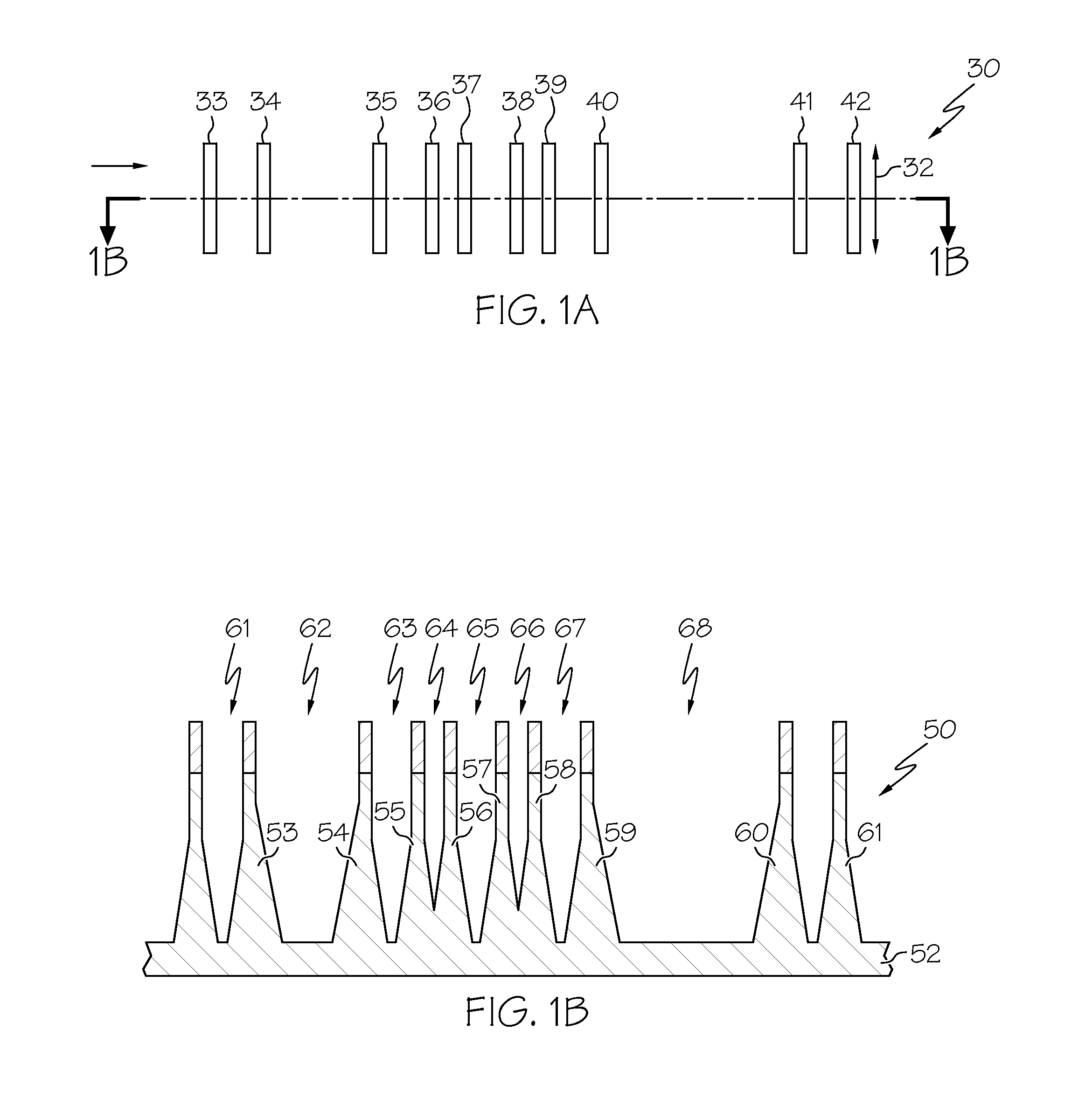
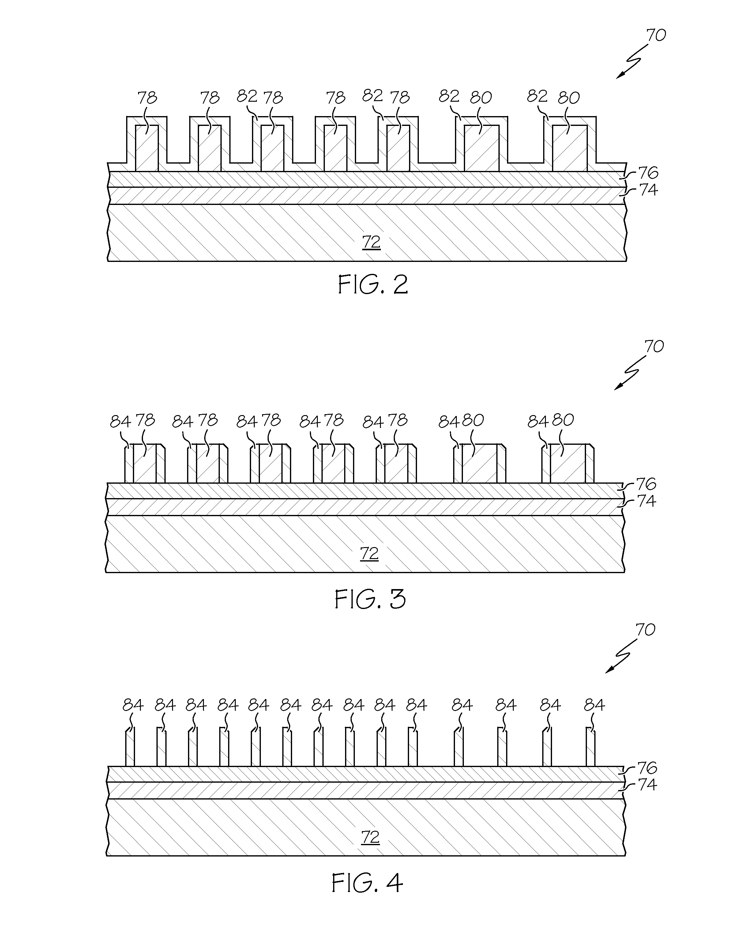
[0012]Methods are provided for the fabrication of FinFET integrated circuits (ICs) in accordance with various embodiments. The embodiments described and illustrated below will find application in ICs of all sizes, but are particularly useful in the fabrication of large ICs such as those that incorporate both logic circuits (which will likely vary greatly from design to design and across a design) and memory circuits such as static random access memory (SRAM) circuits (that will likely be very uniform across a design and from design to design). The memory circuit portion of an IC is fabricated in an array of fins and is somewhat tolerant of...
PUM
 Abstract
Description
Claims
Application Information