Buffer layer structure for light-emitting diode

a buffer layer and diode technology, applied in the field of light-emitting diodes, can solve the problems of single layer defects becoming channels for ion migration, undetectable light-emitting efficiency, and degrading so as to effectively block ion diffusion and enhance light-emitting efficiency of led

Inactive Publication Date: 2013-12-12
HIGH POWER OPTO
View PDF25 Cites 0 Cited by
  • Summary
  • Abstract
  • Description
  • Claims
  • Application Information

AI Technical Summary

Benefits of technology

[0009]Therefore the primary object of the present invention is to provide a buffer layer structure for an LED. The buffer layer structure of t

Problems solved by technology

As such, light-emitting efficiency is undesirably affected and light-emitting efficiency of the LED is degraded.
Further, a single layer also has defects to become channels for ion migration.
Therefore, the structure of the above disclosure offers unsatisfactor

Method used


Image

  • Buffer layer structure for light-emitting diode
  • Buffer layer structure for light-emitting diode
  • Buffer layer structure for light-emitting diode

Examples


Embodiment Construction

[0019]FIG. 3 shows a schematic diagram of a buffer layer structure for a light-emitting diode (LED) according to an embodiment of the present invention. The buffer layer structure is applied to an LED 100. The LED 100 comprises a

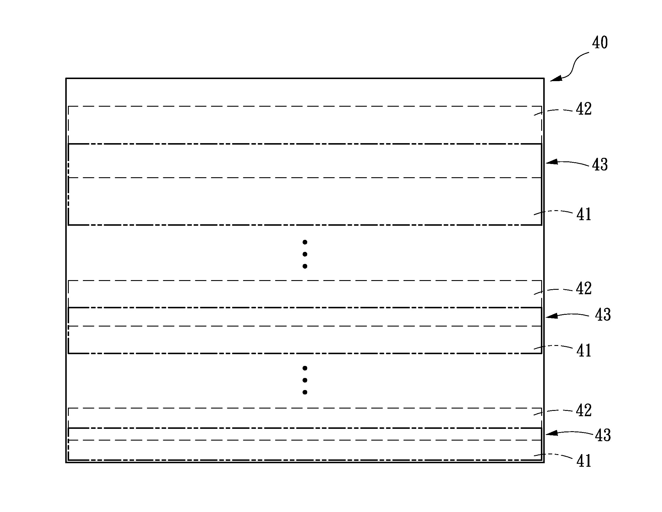
[0020]P-type electrode 10, a permanent substrate 20, a binding layer 30, a buffer layer 40, a mirror layer 50, a P-type semiconductor layer 60, a light-emitting layer 70, an N-type semiconductor layer 80, and an N-type electrode 90 that are stacked in sequence.

[0021]Referring to FIG. 4, the buffer layer 40 of the present invention is a composite material, which includes at least two materials. More specifically, the buffer layer 40 comprises at least one first material 41 and at least one second material 42 that are alternately stacked. One first material 41 and one second material 42 are jointed to become a group 43, and a total thickness of one first material 41 and one second material 42 is regarded as a group thickness (i.e., the thickness of the group 4...


PUM


Abstract

A buffer layer structure for an LED is provided. The LED includes a P-type electrode, a permanent substrate, a binding layer, a buffer layer, a mirror layer, a P-type semiconductor layer, a light-emitting layer, an N-type semiconductor layer, and an N-type electrode that are stacked in sequence. The buffer layer is a composite material, and includes at least one first material and at least one second material that are alternately stacked. The first material and the second material are mutually diffused to generate gradient variation after the buffer layer is processed by a thermal treatment. Thus, an interface effect and thermal stress between difference interfaces are eliminated, and a channel for ion diffusion is blocked for enhancing light-emitting efficiency of the LED.

Description

[0001]This application is a continuation-in-part, and claims priority, of from U.S. patent application Ser. No. 13 / 472,141 filed on May 15, 2012, entitled “TENSION RELEASE LAYER STRUCTURE OF LIGHT-EMITTING DIODE”, the entire contents of which are hereby incorporated by reference.FIELD OF THE INVENTION[0002]The present invention relates to a light-emitting diode (LED), and particularly to an LED for enhancing light-emitting efficiency.BACKGROUND OF THE INVENTION[0003]Referring to FIG. 1, a conventional vertical LED includes a sandwich structure formed by an N-type semiconductor layer 1, a light-emitting layer 2 and a P-type semiconductor layer 3. Below the P-type semiconductor layer 3, a mirror layer 4, a buffer layer 5, a binding layer 6, a silicon substrate 7 and a P-type electrode 8 are formed in sequence. A surface of the N-type semiconductor layer 1 is processed by a roughening treatment for increasing light extraction. An[0004]N-type electrode 9 is further provided. By applying...

Claims


Application Information

Patent Timeline
IPC IPC(8): H01L33/40
CPCH01L33/40H01L33/405H01L33/32H01L33/0079H01L33/0093
Inventor CHOU, LI-PINGYEN, WEI-YUCHEN, FU-BANGCHANG, CHIH-SUNG
Owner HIGH POWER OPTO
Why Eureka
Try Eureka