
Carrier and method for fabricating coreless packaging substrate

a coreless packaging and carrier technology, applied in the direction of conductive pattern formation, printed circuit non-printed electric components, semiconductor/solid-state device details, etc., can solve the problems of increasing the length of the conductive path and the overall structure, not meeting the high performance and miniaturization requirements of electronic products, adversely affecting the product yield, etc., to prevent accumulation of too much stress, prevent warpage of the packaging substrate, and increase the product yield

Active Publication Date: 2013-12-19
UNIMICRON TECH CORP
View PDF4 Cites 6 Cited by
  • Summary
  • Abstract
  • Description
  • Claims
  • Application Information

AI Technical Summary

Benefits of technology

The present invention is about a carrier used in the semiconductor industry to prevent warping of a packaging substrate during processing. The invention only forms a portion of the built-up structure, called the inner built-up circuit board, on the carrier to reduce stress accumulation. The carrier can be reused, saving fabrication costs and reducing waste. Additionally, the invention removes the carrier and symmetrically forms built-up structures on both sides of the circuit board to offset stresses and prevent warping. Overall, this invention improves the production of semiconductor devices and increases yield.

Problems solved by technology

However, the use of the core board increases the length of the conductive path and the thickness of the overall structure, and consequently does not meet high performance and miniaturization requirements of electronic products.
However, since the cutting process is performed to the carrier after the built-up structure has been formed on the carrier, great stresses accumulated in the packaging substrate can easily cause warpage of the packaging substrate, thus adversely affecting the product yield.
Further, the carrier cannot be repeatedly used in the same fabrication process due to the cutting process.

Method used


Image

  • Carrier and method for fabricating coreless packaging substrate
  • Carrier and method for fabricating coreless packaging substrate
  • Carrier and method for fabricating coreless packaging substrate

Examples


Embodiment Construction

[0024]The following illustrative embodiments are provided to illustrate the disclosure of the present invention, these and other advantages and effects can be apparent to those in the art after reading this specification.

[0025]It should be noted that the drawings are only for illustrative purposes and not intended to limit the present invention. Meanwhile, terms such as “top”, “bottom”, “on” etc. are only used as a matter of descriptive convenience and not intended to have any other significance or provide limitations for the present invention.

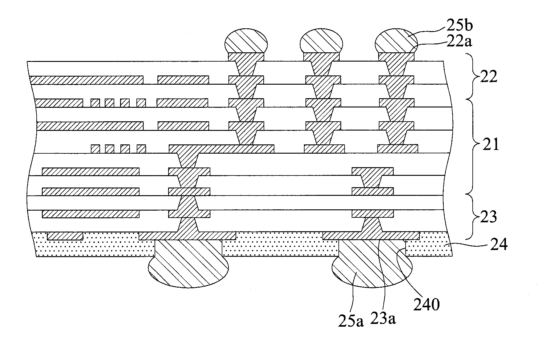
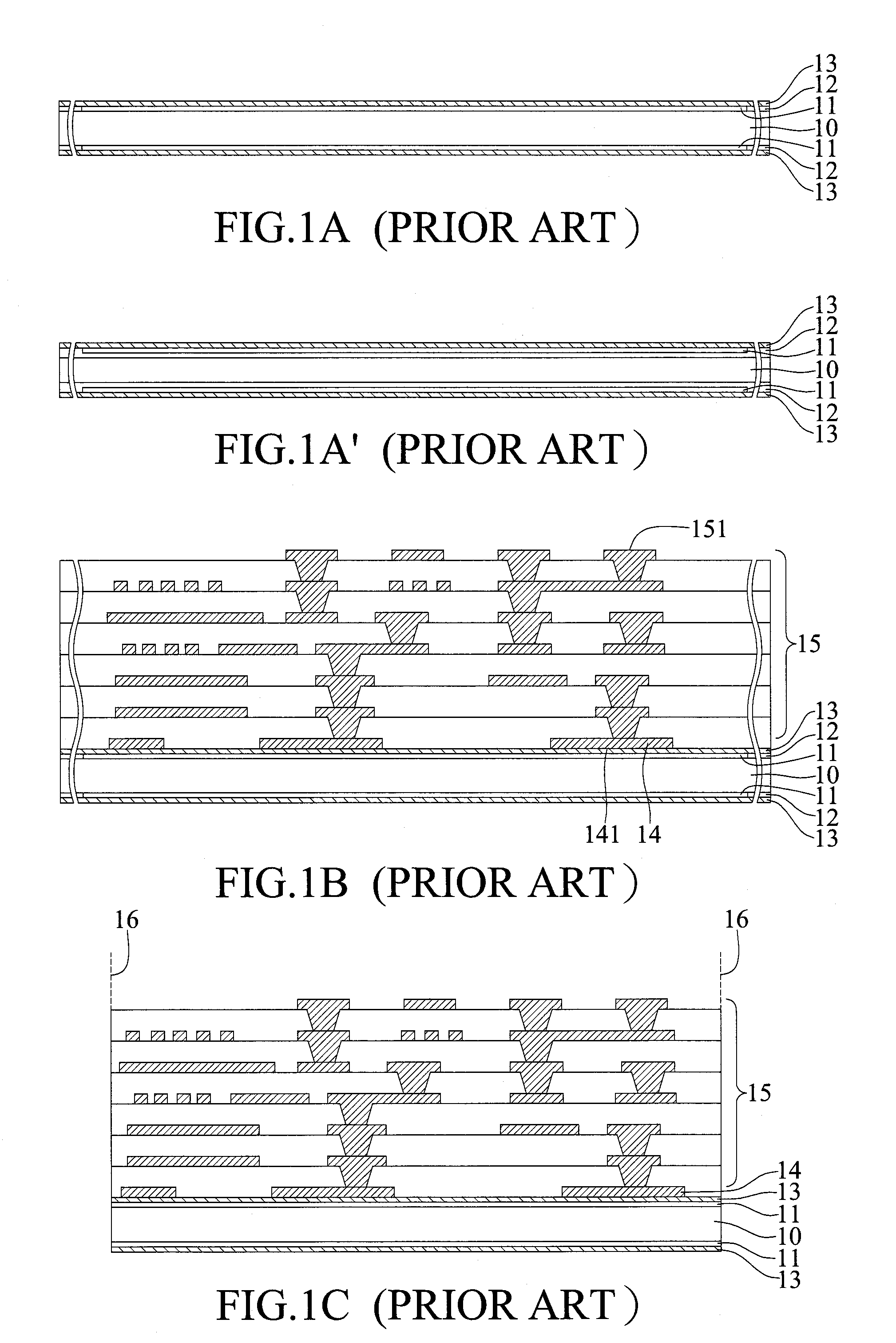
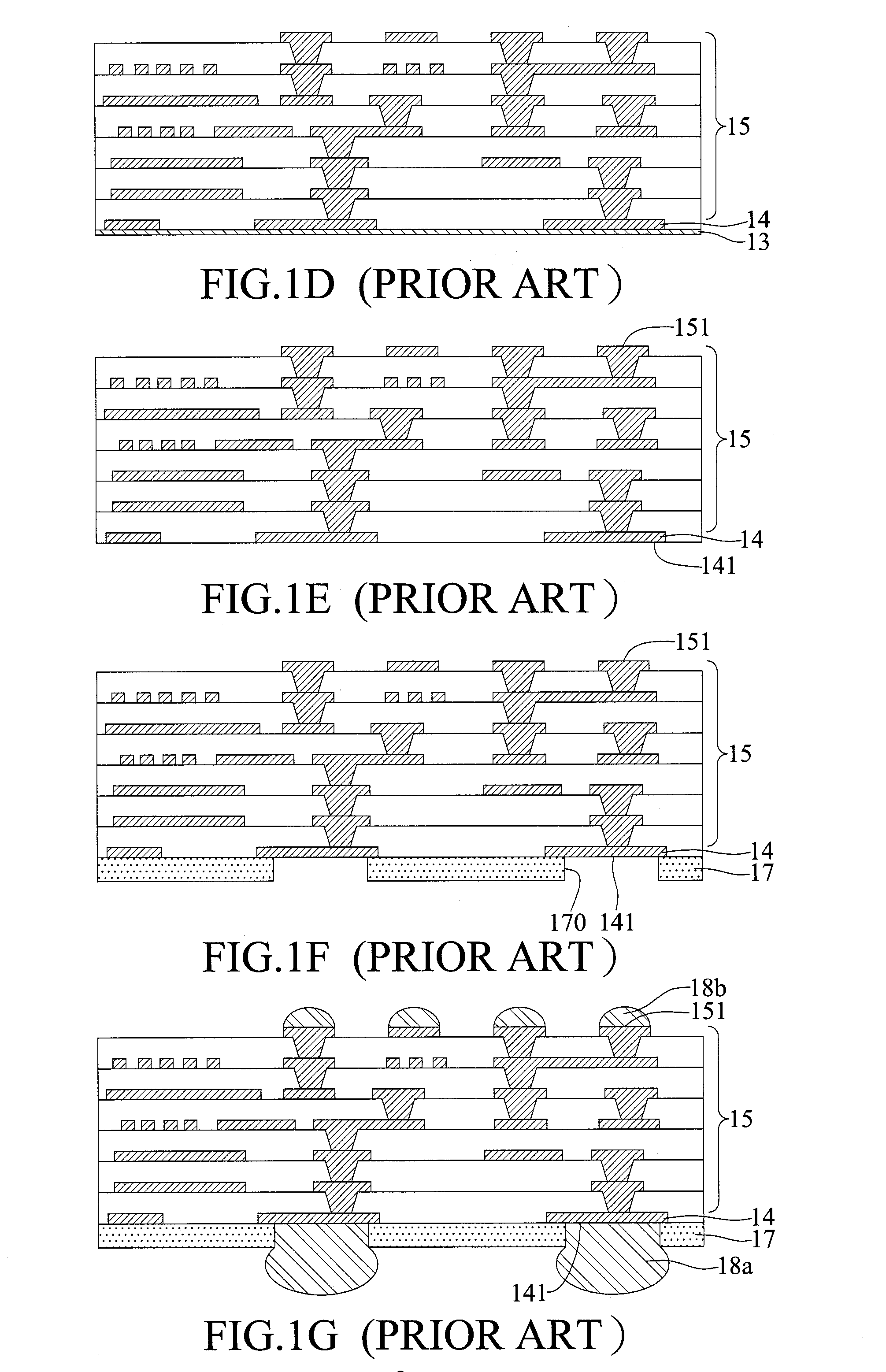
[0026]FIGS. 2A to 2H are schematic cross-sectional views showing a carrier and a method for fabricating a coreless packaging substrate according to the present invention, wherein FIGS. 2A′ and 2A″ show other embodiments of FIG. 2A.

[0027]Referring to FIG. 2A, a carrier 20 is provided. The carrier 20 has a carrying board 200, a release layer 201 formed on each of two opposite surfaces of the carrying board 200, and a first metal layer 202 formed...


PUM

PropertyMeasurementUnit
thicknessaaaaaaaaaa
thicknessaaaaaaaaaa
thicknessaaaaaaaaaa

Abstract

A fabrication method of a coreless packaging substrate is provided, including the steps of: forming an inner built-up circuit board on a carrier; removing the carrier; and symmetrically forming a first outer built-up structure and a second outer built-up structure on top and bottom surfaces of the inner built-up circuit board, respectively. The present invention effectively increases the product yield, saves the fabrication cost, and reduces wastes.

Description

BACKGROUND OF THE INVENTION[0001]1. Field of the Invention[0002]The present invention relates to carriers and fabrication methods of coreless packaging substrates, and, more particularly, to a carrier and a method for fabricating a coreless packaging substrate using the same.[0003]2. Description of Related Art[0004]Along with the rapid development of electronic industries, electronic products are developed towards multi-function and high performance. Accordingly, different types of packages, such as wire bonding or flip-chip packages, have been developed. To meet high integration and miniaturization requirements of semiconductor packages, packaging substrates are developed from single layer circuit boards to multi-layer circuit boards so as to provide more spaces for circuit layout in a limited area by using interlayer connection technologies and reduce the thickness of the packaging substrates.[0005]A conventional packaging substrate has a core board having circuits formed thereon,...

Claims


Application Information

Patent Timeline
Patent Type & Authority Applications(United States)
IPC IPC(8): H05K3/10H05K1/02
CPCH05K3/10H05K1/02H01L23/145H05K1/0271H05K3/4682H01L23/49811H01L23/49827H01L21/568H01L2924/0002Y10T29/49155H01L2924/00H05K1/05H05K3/4644
Inventor TSENG, TZYY-JANGHO, CHUNG W.HU, DYI-CHUNGLEE, HUAN-LINGHE, SHENG-YUAH
Owner UNIMICRON TECH CORP
Learn More