Light emitting diode dielectric mirror

a technology of dielectric mirrors and light emitting diodes, which is applied in the direction of basic electric elements, electrical equipment, semiconductor devices, etc., can solve the problems of light being absorbed by the reflector cup, optical loss may occur when the light is reflected, and limited external quantum efficiency, etc., to achieve the effect of increasing emission efficiency

Active Publication Date: 2013-12-26
CREELED INC
View PDF7 Cites 29 Cited by
  • Summary
  • Abstract
  • Description
  • Claims
  • Application Information

AI Technical Summary

Benefits of technology

[0012]The present invention discloses one or more reflectivity layers for use in LEDs and LED chips to increase emission efficiency. One embodiment of a LED chip according to the present invention comprises an active LED structure having an active layer between two oppositely doped layers, and the active layer emitting light in response to an electrical signal applied to the oppositely doped

Problems solved by technology

For conventional LEDs with a single out-coupling surface, the external quantum efficiency can be limited by a number of factors, such as total internal reflection (TIR) of light from the LED's emission region.
While the reflective cup 13 may direct light in an upward direction, optical losses may occur when the light is reflected.
Some light may be absorbed by the reflector cup due to the less than 100% reflectivity of

Method used


Image

  • Light emitting diode dielectric mirror
  • Light emitting diode dielectric mirror
  • Light emitting diode dielectric mirror

Examples


Embodiment Construction

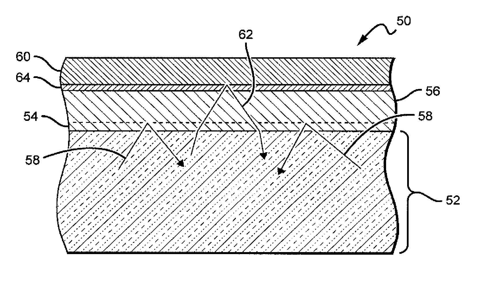
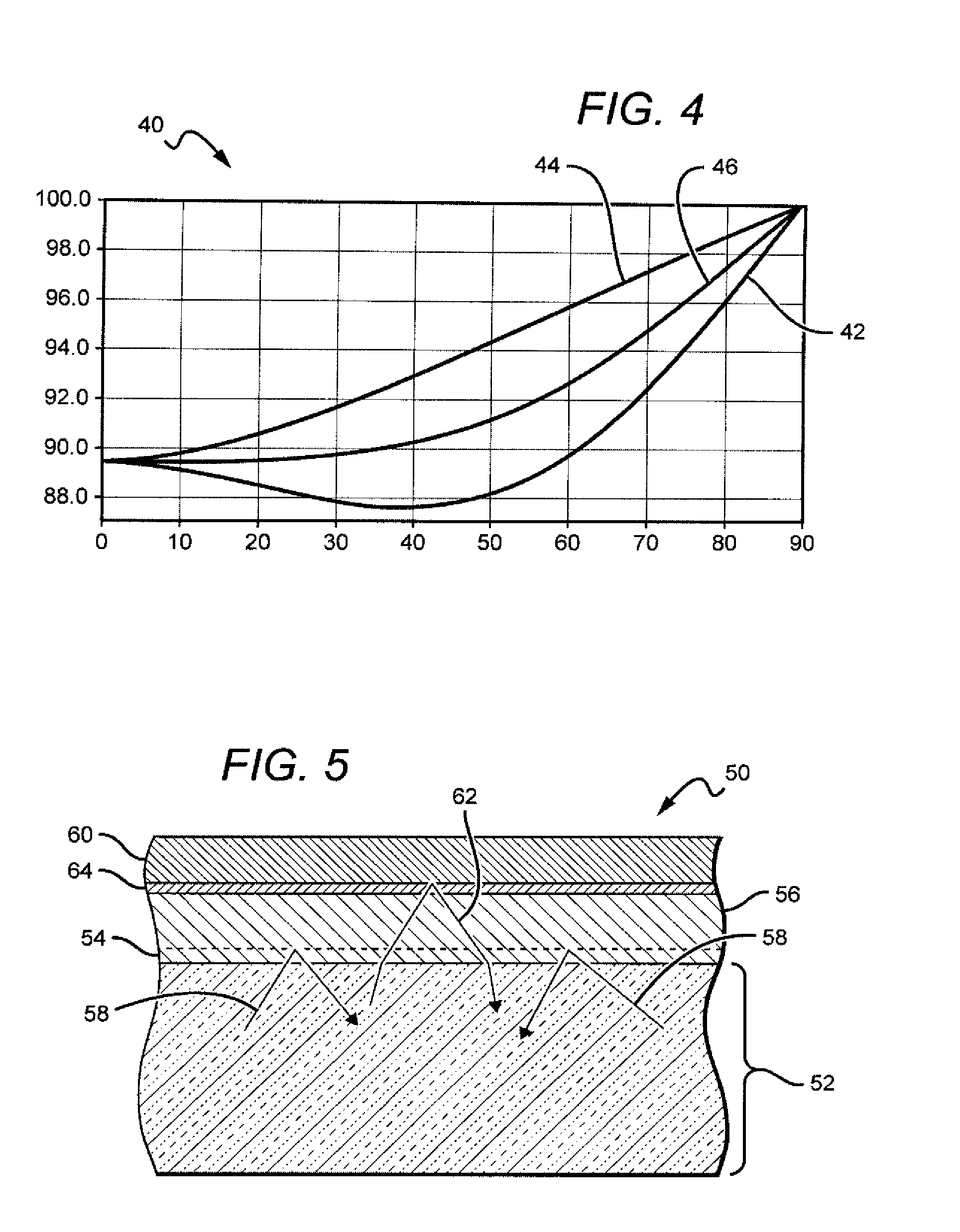
[0023]The present invention is directed to solid-state emitters having internal or integral reflective surfaces / layers arranged to increase the emission efficiency of the emitters. The present invention is described herein with reference to light emitting diodes (LED or LEDs) but it is understood that it is equally applicable to other solid-state emitters. The present invention can be used as a reflector in conjunction with one or more contacts, or can be used as a reflector separate from the contacts.

[0024]As described above, different embodiments of light emitting diode (LED) chips according to the present invention comprises an active LED structure having an active layer between two oppositely doped layers. A first reflective layer can be provided adjacent to a one of the oppositely doped, layers, with the first layer comprising a material with a different index of refraction than the active LED structure. In most embodiments, the first layer can comprise a layer with an IR that ...


PUM


Abstract

A high efficiency LED chip is disclosed that comprises an active LED structure comprising an active layer between two oppositely doped layers. A first reflective layer can be provided adjacent to one of the oppositely doped layers, with the first layer comprising a material with a different index of refraction than the active LED structure. The difference in IR between the active LED structure and the first reflective layer increases TIR of light at the junction. In some embodiments the first reflective layer can comprise an IR lower than the semiconductor material, increasing the amount of light that can experience TIR. Some embodiments of LED chips according to the present invention can also comprise a second reflective layer or metal layer on and used in conjunction with the first reflective layer such that light passing through the first reflective layer can be reflected by the second reflective layer.

Description

[0001]This application is a continuation of, and claims the benefit of, U.S. patent application Ser. No. 13 / 071,349, to Ibbetson, et al., filed on Mar. 24, 2011, which is a continuation of and claims the benefit of U.S. patent application Ser. No. 12 / 316,097, to Li, et al., filed on Dec. 8, 2008. This application is also a continuation of, and claims the benefit of, U.S. patent application Ser. No. 12 / 463,709, to Denofrio, et al., filed on May 11, 2009, which is also a continuation-in-part of U.S. patent application Ser. No. 11 / 985,410, to Keller, et al., filed on Nov. 14, 2007, and a continuation-in-part of U.S. patent application Ser. No. 12 / 329,713, to Denofrio, et al. filed on Dec. 8, 2008.BACKGROUND OF THE INVENTION[0002]1. Field of the Invention[0003]This invention relates to light emitting diodes, and more particularly to light emitting diodes having high reflectivity mirrors.[0004]2. Description of the Related Art[0005]Light emitting diodes (LED or LEDs) are solid state devi...

Claims


Application Information

Patent Timeline
IPC IPC(8): H01L33/10H01L33/32
CPCH01L33/10H01L33/32H01L33/46H01L33/38H01L33/405
Inventor HEIKMAN, STENIBBETSON, JAMES
Owner CREELED INC
Why Eureka
Try Eureka