Integrated electronic device for monitoring parameters within a solid structure and monitoring system using such a device

a technology of integrated electronic devices and solid structures, which is applied in the direction of measuring devices, material analysis through electric/magnetic means, instruments, etc., can solve the problems of only being applied after the structure is built, devices are not able to exhaustively detect the parameters within the structure to be monitored, and cannot evaluate possible initial defects

Active Publication Date: 2013-12-26
STMICROELECTRONICS SRL
View PDF6 Cites 27 Cited by
  • Summary
  • Abstract
  • Description
  • Claims
  • Application Information

AI Technical Summary

Problems solved by technology

Such devices are not however able to exhaustively detect the parameters within the structure to be monitored, which it is very useful to know in order to evaluate the quality of the structure, its safety, its ageing, its reaction to variable atmospheric conditions, and so on.
Moreover, such devices can only be applied after the structure has been built, and not while it is being built.
Therefore, they are unable to evaluate possible initial defects.
There are also numerous other causes of wearing, over time, due for example to water infiltration, capable of damaging the system.
A drawback of known systems, like the system of U.S. Pat. No. 6,950,767, derives from the fact that they are complex systems, even though they are enclosed in a package, and can therefore be damaged when facing the operating conditions in which they must work.
In particular, the electrical interconnections between the various parts of the SiP of U.S. Pat. No. 6,950,767 can be ...

Method used


Image

  • Integrated electronic device for monitoring parameters within a solid structure and monitoring system using such a device
  • Integrated electronic device for monitoring parameters within a solid structure and monitoring system using such a device
  • Integrated electronic device for monitoring parameters within a solid structure and monitoring system using such a device

Examples


Embodiment Construction

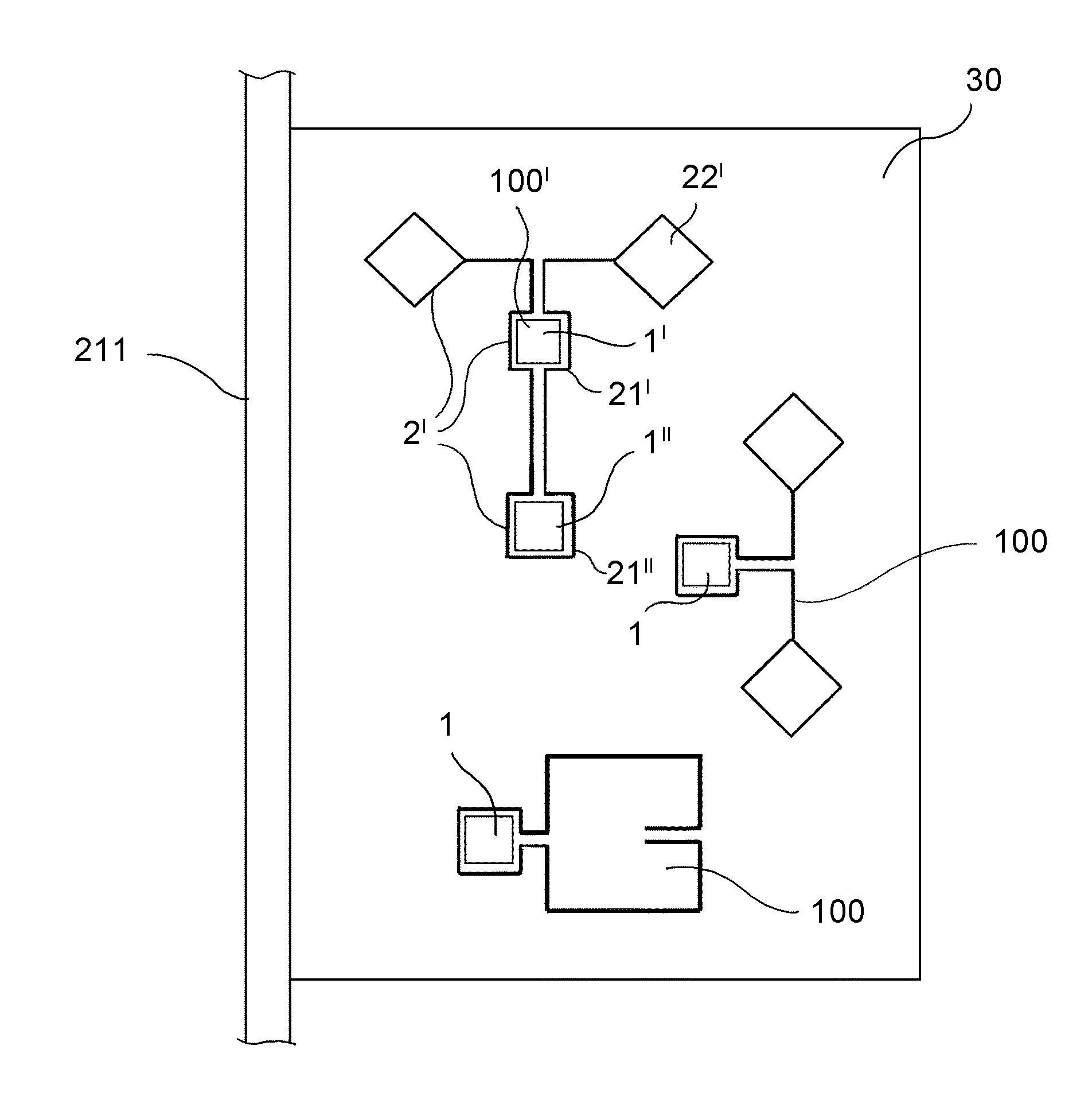
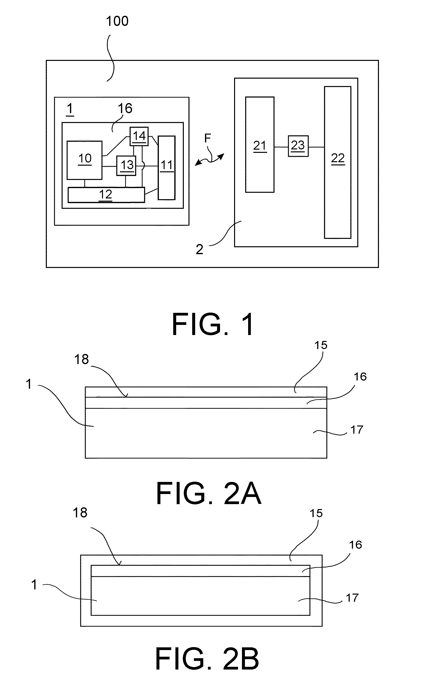
[0041]With reference to FIG. 1, an electronic device 100 for detecting and monitoring one or more local parameters within a solid structure is described (which device henceforth we will define as “monitoring device” for the sake of brevity), according to an example of the present invention.

[0042]The monitoring device 100 comprises an integrated detection module 1, made on a single semiconductor chip (henceforth defined simply as chip), wherein the semiconductor is, typically, silicon.

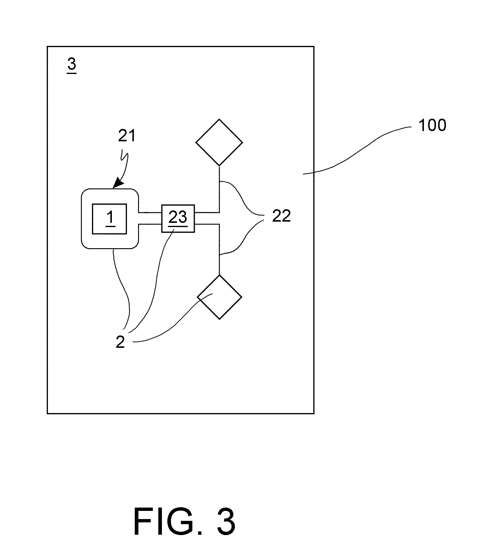
[0043]The monitoring device 100 also comprises, fixedly connected to the integrated detection module 1, electromagnetic means 2 for transmitting / receiving telecommunications signals and exchanging energy between the integrated detection module 1 and an external control and data collection system, not shown in FIG. 1.

[0044]The integrated detection module 1 comprises an integrated functional circuitry portion 16. For the purposes of the present description, by the term “integrated functional circuitry por...


PUM


Abstract

Device (100) for detecting and monitoring local parameters within a solid structure (300). The device comprises an integrated detection module (1) made on a single chip, having an integrated functional circuitry portion (16) comprising at least one integrated sensor (10) and an integrated antenna (11), and electromagnetic means (2) for transmitting/receiving signals and energy exchange. The integrated functional circuitry portion (16) comprises a functional surface (18) facing towards the outside of the chip. A passivation layer (15) is arranged to completely cover at least the functional surface (18), so that the integrated detection module (1) is entirely hermetically sealed and galvanically insulated from the surrounding environment. The integrated antenna (11), the electromagnetic means (2) and the remote antenna (221) are operatively connected wirelessly through magnetic or electromagnetic coupling.

Description

TECHNOLOGICAL BACKGROUND OF THE INVENTION[0001]1. Field of Application[0002]The present invention refers to integrated electronic devices for monitoring parameters within a solid structure, and in particular to a device for detecting and monitoring parameters in accordance with the preamble of claim 1.[0003]The present invention also comprises a system for monitoring parameters, within a solid structure, which uses the aforementioned integrated electronic device for monitoring parameters.[0004]2. Description of the Prior Art[0005]In solid structures, particularly in load-bearing structures of, for example, bridges, buildings, tunnels, railways, containment walls, dams, embankments, pipelines and underground structures of metropolitan transport lines, and so on, it is very important to monitor, in many points, significant parameters, like for example pressure, temperature and mechanical stresses.[0006]Such monitoring, carried out periodically or continuously, is useful both at the in...

Claims


Application Information

Patent Timeline
IPC IPC(8): G01N27/00
CPCG01N27/00G01M5/0083G01L1/26
Inventor PAGANI, ALBERTOMURARI, BRUNO
Owner STMICROELECTRONICS SRL
Why Eureka
Try Eureka