Variable capacitance element and tunable filter

Active Publication Date: 2013-12-26
MURATA MFG CO LTD
View PDF8 Cites 21 Cited by
  • Summary
  • Abstract
  • Description
  • Claims
  • Application Information

AI Technical Summary

Benefits of technology

[0036]In a variable capacitance element according to a preferred embodiment of the present invention, a dielectric layer whose relative dielectric constant varies in accordance with an applied voltage is located on a piezoelectric substrate with a buffer layer having an orientation interposed therebetween, and first and second electrodes are arranged to apply an electric field to the dielectric layer. Accordingly, the variable capacitance element that is located o

Problems solved by technology

Further, the deposition temperature of BST is as high as 800° C. to 900° C. Therefore, if a BST film is to be formed on a piezoelectric substrate that is formed of a piezoelectric material having a low Curie temperature, there is a risk of the piezoelectric characteristics thereof being degraded.
Further, there are also such problems as the piezoelectric substrate warping or

Method used


Image

  • Variable capacitance element and tunable filter
  • Variable capacitance element and tunable filter
  • Variable capacitance element and tunable filter

Examples


Example

[0082]With reference to Example 1 and Example 2, it will be described below that tendencies of changes in tan δ and in the relative dielectric constant in accordance with an applied voltage vary depending on the crystal structure and the orientation direction of the buffer layer.

EXAMPLE 1

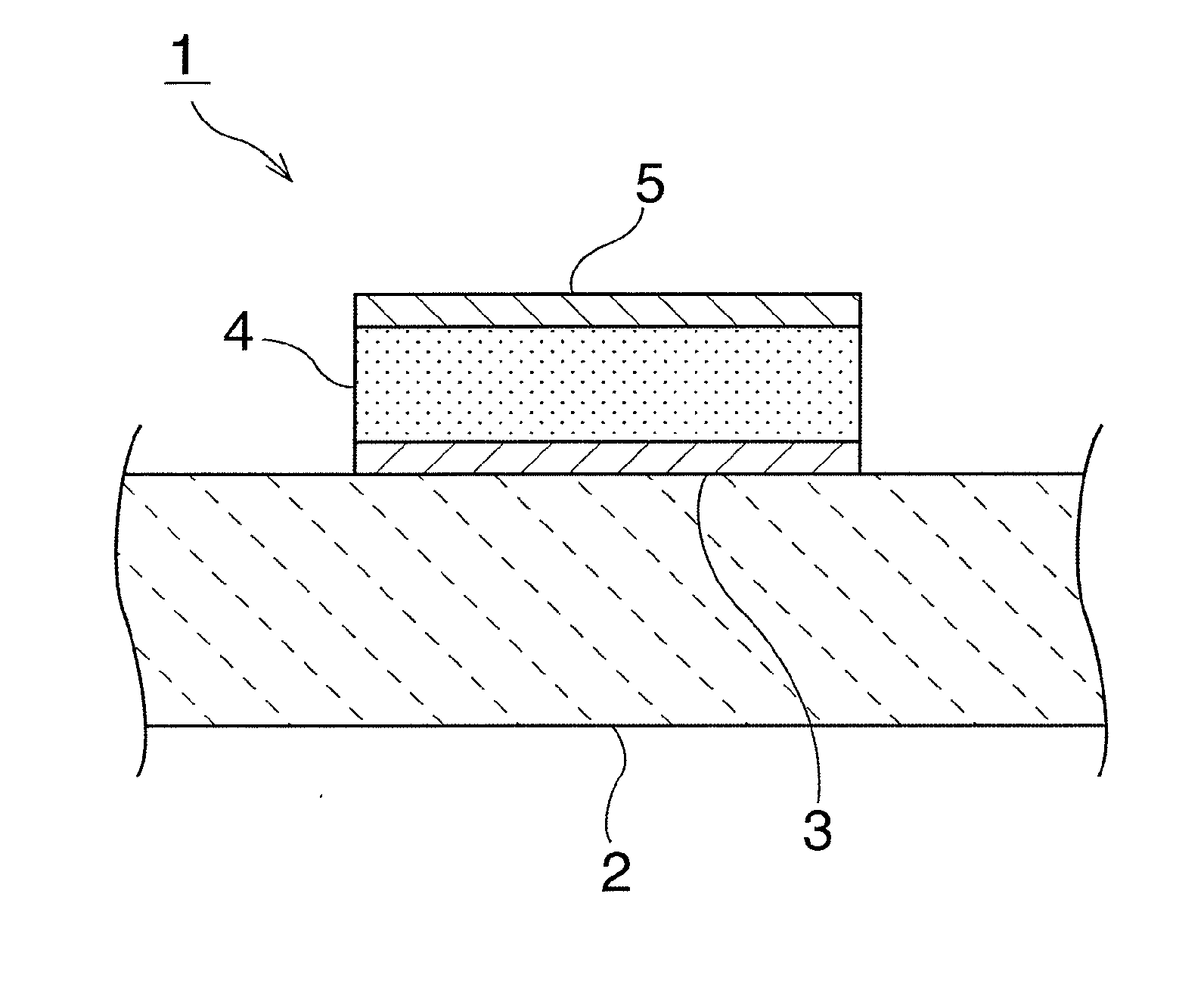
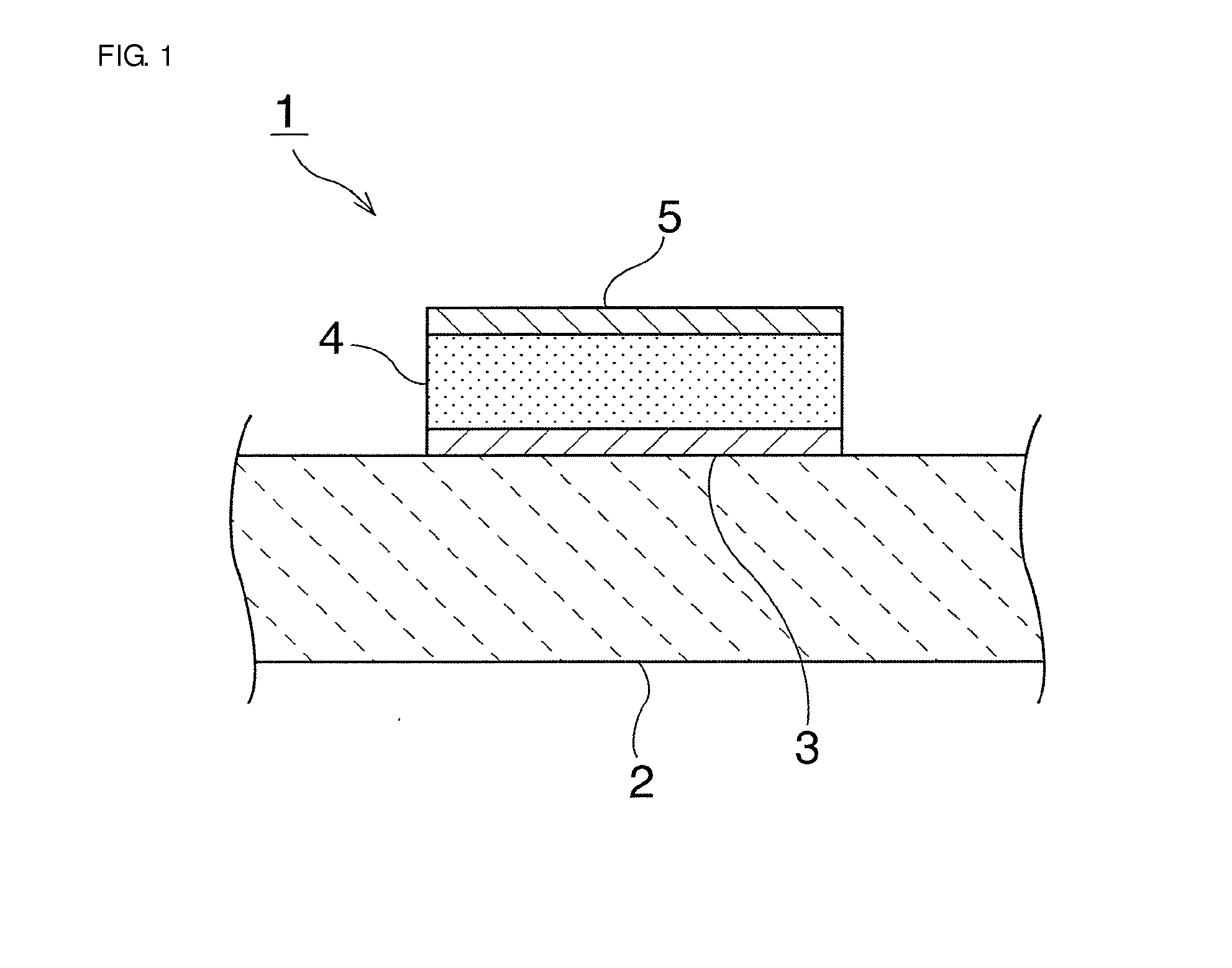
[0083]A buffer layer 3 having a cubic crystal structure and formed of a Pt(111) film was deposited in a thickness of 100 nm on a piezoelectric substrate 2 formed of 15° Y cut LiNbO3 through sputtering using an Ar gas at a substrate temperature of 400° C. A dielectric layer 4 formed of BaSrTiO3 was then formed on the buffer layer 3 through sputtering at a temperature of 700° C. A second electrode 5 formed of Pt was then formed as a film in a thickness of 200 nm on the dielectric layer 4 through sputtering to obtain a variable capacitance element 1. Relationships between a dielectric constant and an applied voltage and between tan δ and the applied voltage in this variable capacitance element are illu...

Example

EXAMPLE 2

[0088]Similarly to Example 1, but a Pt(200) film having a cubic crystal structure was deposited as the buffer layer 3. The deposition conditions were as follows. The buffer layer 3 was deposited in a film thickness of 100 nm through sputtering using an Ar gas at a substrate temperature of 700° C.

[0089]Other points were the same as in those in Example 1.

[0090]Relationships between a relative dielectric constant and an applied voltage and between tan δ and the applied voltage in the variable capacitance element obtained through Example 2 are illustrated in FIG. 4. FIG. 4 clearly reveals that the relative dielectric constant and tan δ changed more greatly than in Example 1 as the applied voltage changed. The rate of change in the relative dielectric constant, which is a ratio of the highest relative dielectric constant to the lowest relative dielectric constant within a range where the applied voltage is between −5 V and +5 V, was 4.17. Accordingly, it was discovered that a va...

Example

EXAMPLE 3

[0092]The buffer layer 3 having a cubic crystal structure and including the Pt(111) film was formed on the piezoelectric substrate that is formed of −1° Y cut LiNbO3, and a variable capacitance element was obtained thereafter in a similar manner to Example 1. The Pt(111) film was deposited in a film thickness of 100 nm through sputtering using an Ar gas at a substrate temperature of 400° C.

[0093]Relationships between a relative dielectric constant and an applied voltage and between tan δ and the applied voltage in the variable capacitance element obtained through Example 3 are illustrated in FIG. 8. FIG. 8 clearly reveals that as the applied voltage changed, the relative dielectric constant and tan δ also changed.

[0094]Further, the rate of change in the relative dielectric constant within a range where the applied voltage is between −5 V and +5 V was 3.34, which was greater than in Example 1 but smaller than in Example 2.

[0095]As for the variable capacitance element of Exam...


PUM


Abstract

A variable capacitance element includes a piezoelectric substrate, a buffer layer located on the piezoelectric substrate with an orientation, a dielectric layer located on the buffer layer and having a relative dielectric constant that varies in accordance with an applied voltage, and a first electrode and a second electrode arranged to apply an electric field to the dielectric layer.

Description

BACKGROUND OF THE INVENTION[0001]1. Field of the Invention[0002]The present invention relates to a variable capacitance element that includes a dielectric layer whose relative dielectric constant varies in accordance with an applied voltage, and in particular, relates to a variable capacitance element that includes such a dielectric film and that is provided on a piezoelectric substrate, and to a tunable filter that includes the variable capacitance element.[0003]2. Description of the Related Art[0004]To date, a variable capacitance element whose capacitance can be varied has been widely used in an electronic component. As such a variable capacitance element, Japanese Unexamined Patent Application Publication No. 11-260667 discloses, for example, a variable capacitance element in which a barium strontium titanate film is formed as a dielectric layer on a ceramic substrate.[0005]Meanwhile, for mobile communication devices such as a cellular phone, there is a strong demand for reducin...

Claims


Application Information

Patent Timeline
IPC IPC(8): H03H9/54H03H9/64H01G7/06
CPCH01G7/06H03H9/542H03H9/64H03H9/6403H03H2003/0464H03H2009/02165
Inventor KADOTA, MICHIOKOUTSAROFF, IVOYL P.KIMURA, TETSUYATOCHISHITA, HIKARI
Owner MURATA MFG CO LTD
Why Eureka
Try Eureka