
Dielectric for carbon-based nano-devices

a carbon-based nano-device and dielectric technology, applied in the direction of nano-devices, semiconductor devices, electrical devices, etc., can solve the problems of graphene-channel devices and subsequent deposition of insulating layers,

Inactive Publication Date: 2014-01-02
IBM CORP
View PDF2 Cites 12 Cited by
  • Summary
  • Abstract
  • Description
  • Claims
  • Application Information

AI Technical Summary

Benefits of technology

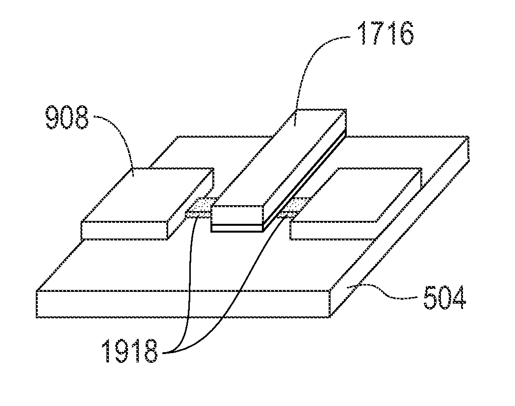
This patent describes a carbon-based semiconductor device and a program for fabricating it. The device has a substrate, source / drain contacts, a graphene channel, a dielectric layer, and a gate contact. The gate contact is in a non-overlapping position with the source and drain contacts, leaving exposed sections of the graphene channel between the gate contact and the source / drain contacts. The technical effect of this design is to allow for better control of the electrical properties of the semiconductor device, resulting in improved performance.

Problems solved by technology

However, fabrication of a graphene-channel device depends on finding a suitable dielectric.
It follows that out-of-plane bonding is suppressed, making subsequent deposition of an insulating layer problematic.

Method used


Image

  • Dielectric for carbon-based nano-devices
  • Dielectric for carbon-based nano-devices
  • Dielectric for carbon-based nano-devices

Examples


Embodiment Construction

[0029]Fabrication of a graphene channel FET requires a graphene (Gr) channel and a gate conductor with an intervening gate dielectric. The gate dielectric needs stop charge from leaking between the gate and the channel, and the dielectric should not contain charge internally. Dielectric (insulating) layers are difficult to deposit on a graphene channel because the carbon atoms in graphene have all their bonds to neighboring carbon atoms. Thus, there are no dangling bonds to nucleate growth of the insulating layer. Methods have been used to overcome this problem, such as use of a metal seed layer to promote growth, or deposition of an organic adhesion layer prior to insulator growth. In the former case, the shortcoming of the seed layer is that metal ions disrupt the graphene lattice, or serve as charged centers for carrier scattering, thus lowering the carrier mobility in graphene channel. Furthermore, it is difficult to insure that the metal seed layer does not migrate and form isl...


PUM


Abstract

A carbon-based semiconductor device includes a substrate, source / drain contacts, a graphene channel, a dielectric layer, and a gate. The source / drain contacts are formed on the substrate. The graphene channel is formed on the substrate connecting the source contact and the drain contact. The dielectric layer is formed on the graphene channel with a molecular beam deposition process. The gate contact is formed over the graphene channel and on the dielectric. The gate contact is in a non-overlapping position with the source and drain contacts leaving exposed sections of the graphene channel between the gate contact and the source and drain contacts.

Description

CROSS-REFERENCE TO RELATED APPLICATIONS[0001]This application is a continuation of and claims priority from U.S. patent application Ser. No. 13 / 536,875, Attorney Docket No. YOR920120266US1, filed on Jun. 28, 2012, the entire disclosure of which is herein incorporated by reference.STATEMENT REGARDING FEDERALLY SPONSORED RESEARCH OR DEVELOPMENT[0002]This invention was made with Government support under Contract No.: FA8650-08-C-7838 awarded by Defense Advanced Research Projects Agency (DARPA). The Government has certain rights in this invention.BACKGROUND[0003]The present invention generally relates to carbon-based devices, and more particularly relates graphene-channel based device and techniques for the fabrication thereof. Graphene is a single layer of graphite. Graphene possesses extraordinary electronic properties. For example, the electron carriers in graphene exhibit very high mobilities that are attractive for high-performance circuits. However, fabrication of a graphene-chann...

Claims


Application Information

Patent Timeline
Patent Type & Authority Applications(United States)
IPC IPC(8): H01L29/78H01L21/336B82Y40/00B82Y99/00
CPCB82Y40/00H01L21/02192H01L21/02194H01L21/02269H01L29/0673H01L29/1606H01L29/517H01L29/66045H01L29/778H01L29/7781H01L21/02527
Inventor BOJARCZUK, NESTOR A.COPEL, MATTHEW W.LIN, YU-MING
Owner IBM CORP
Learn More