Semiconductor substrate having high and low-resistivity portions

a technology of resistivity and substrate, applied in the field of electromagnetics, can solve the problems of low resistance and poor free-carrier conduction properties, and achieve the effect of removing parasitic coupling

Inactive Publication Date: 2014-01-02
SKYWORKS SOLUTIONS INC
View PDF2 Cites 26 Cited by
  • Summary
  • Abstract
  • Description
  • Claims
  • Application Information

AI Technical Summary

Benefits of technology

[0010]In certain embodiments, the semiconductor die includes one or more trenches disposed between the RF device and the low-resistivity region. For example, the die may include ...

Problems solved by technology

The semiconductor die may further include a layer of high resistivity amorphous sil...

Method used


Image

  • Semiconductor substrate having high and low-resistivity portions
  • Semiconductor substrate having high and low-resistivity portions
  • Semiconductor substrate having high and low-resistivity portions

Examples


Embodiment Construction

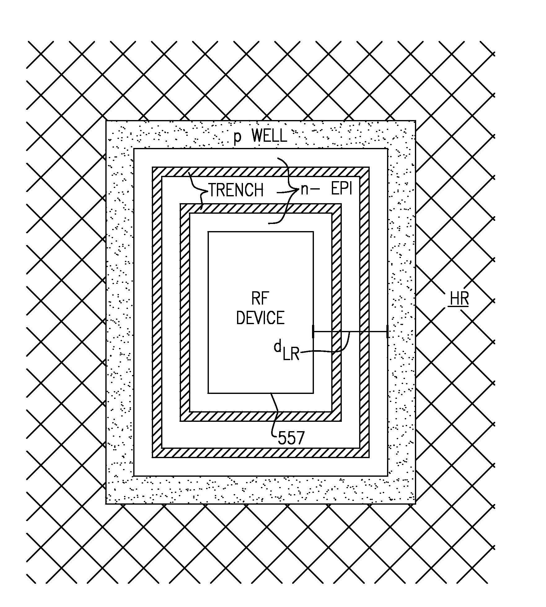
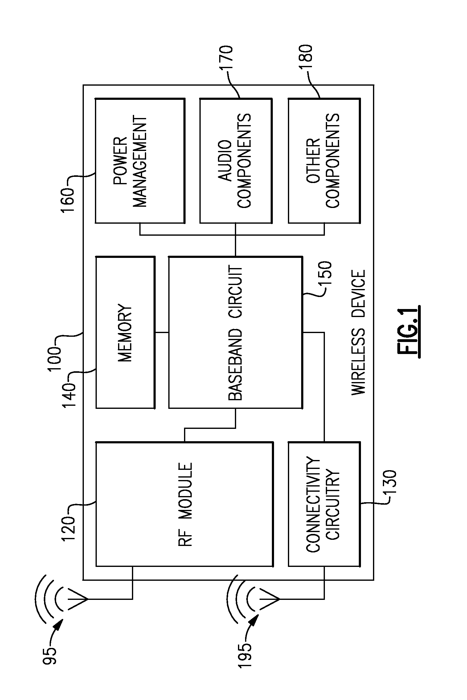
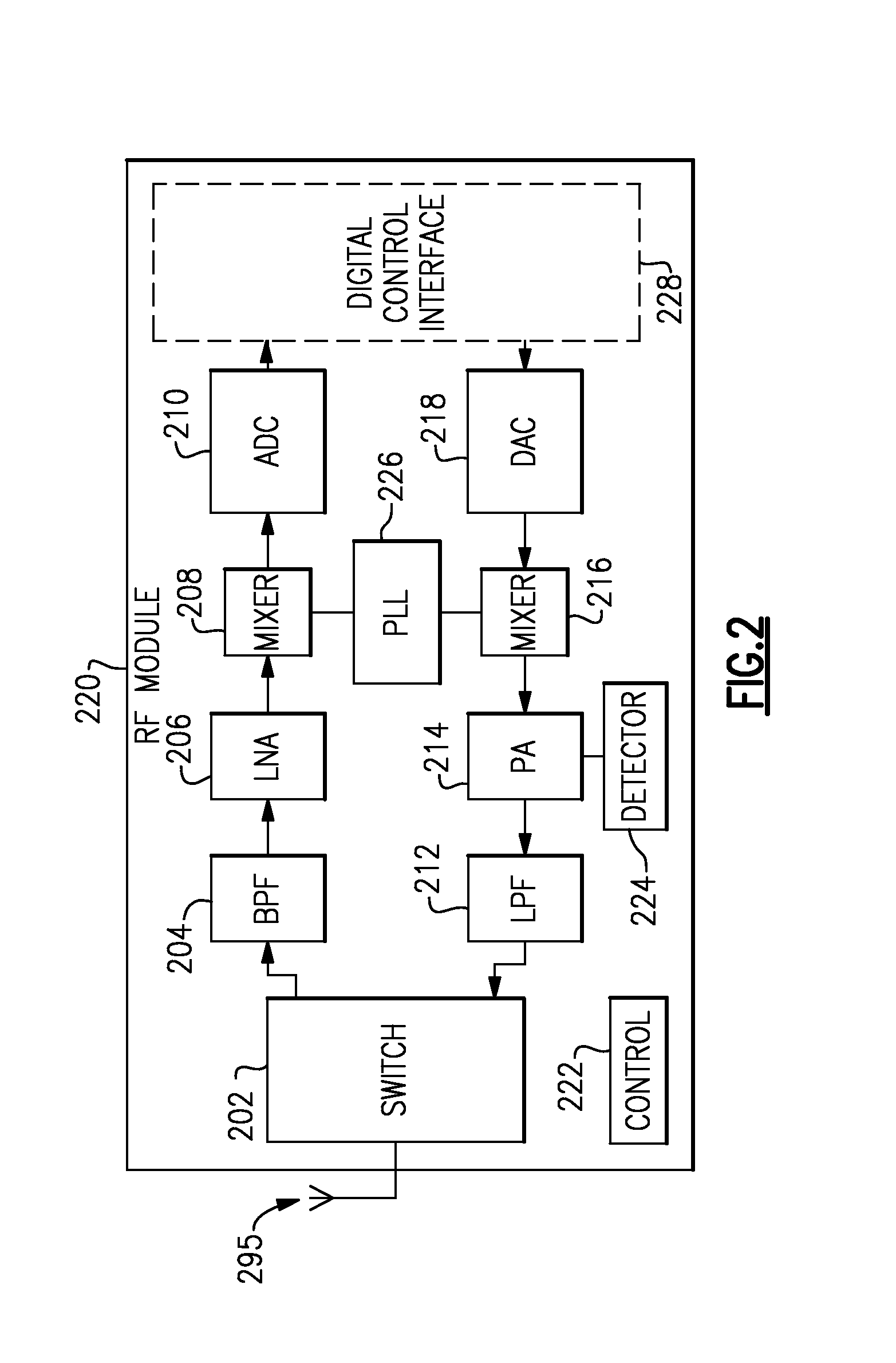
[0032]Disclosed herein are example configurations and embodiments relating to integrated RF front-end modules (FEMs), such as fully-integrated FEM's. For example, embodiments of integrated SiGe BiCMOS FEM's are disclosed that may enable emerging high throughput 802.11ac WLAN applications.

[0033]As discussed above, RF FEM's are incorporated into various types of wireless devices, including computer network radios, cellular phones, PDAs, electronic gaming devices, security and monitoring systems, multi-media systems, and other electronic devices including wireless LAN (WLAN) radios. In the last decade, there have been a number of major trends in the evolution of WLAN radios. For example, with the increasing demand of higher data rate communications, the multiple-input, multiple-output (MIMO) technique has been widely adopted to increase the data rate from the 54 Mbps of a single-input single-output (SISO) operation to 108 Mbps, or more, dual stream MIMO operation. In another example, t...


PUM


Abstract

Systems and methods are disclosed for disposing high and low-resistivity portions of semiconductor substrate in proximity to an active radio frequency (RF) device, thereby at least partially controlling harmonic interference associated with the device. The device may be disposed above the high-resistivity portion, and at least partially surrounded by the low-resistivity portion. The high and low-resistivity portions may provide various benefits associated with interference attenuation, thermal properties, or other benefits. The low-resistivity region can be disposed an optimized distance away from the device.

Description

BACKGROUND[0001]1. Field[0002]The present disclosure generally relates to the field of electronics, and more particularly, to radio frequency front-end modules.[0003]2. Description of Related Art[0004]Radio frequency (RF) is a common term for a range of frequency of electromagnetic radiation typically used to produce and detect radio waves. Such a range can be from about 30 kHz to 300 GHz. Wireless communication devices often include front-end circuitry for processing or conditioning RF signals at an incoming or outgoing frequency or signal port. RF front-end modules may be components of receiver, transmitter, or transceiver systems associated with a wireless device.[0005]RF front-end design may include a number of considerations, including complexity, substrate compatibility, performance, and integration.SUMMARY[0006]Certain embodiments disclosed herein provide a semiconductor die including a silicon substrate having a high-resistivity portion, an active RF device disposed on the s...

Claims


Application Information

Patent Timeline
IPC IPC(8): H01L29/06H01L21/34
CPCH01L21/26506H01L29/78H01L29/7378H01L29/0821H01L21/76H01L27/0823H01L2224/32245H01L2224/4813H01L2224/48137H01L2224/48247H01L2224/48257H01L2224/49111H01L2224/73265H01L2924/181H01L2924/00H01L2924/00012
Inventor MCPARTLIN, MICHAEL JOSEPH
Owner SKYWORKS SOLUTIONS INC
Why Eureka
Try Eureka