
Substrate for LED module and method for manufacturing the same

a technology of led modules and substrates, which is applied in the direction of vacuum evaporation coatings, conductive pattern formation, sputtering coatings, etc., can solve the problems of increasing manufacturing costs, increasing efficiency, and increasing manufacturing costs, so as to improve manufacturing efficiency, simplify manufacturing processes, and improve light reflectivity.

Inactive Publication Date: 2014-01-23
SAMSUNG ELECTRO MECHANICS CO LTD
View PDF0 Cites 18 Cited by
  • Summary
  • Abstract
  • Description
  • Claims
  • Application Information

AI Technical Summary

Benefits of technology

The present invention aims to solve the problems of low light reflectivity in LED modules and offer an easy, cost-effective method to fabricate a substrate for an LED module with excellent light reflectivity.

Problems solved by technology

Particularly, since the PCB for the LED module has directionality, there are problems that an additional member such as a reflection plate or a light guide plate is utilized according to the device mounting shape of the PCB for the LED module during the manufacture thereof.
That is, if the LED device is mounted on the PCB for the conventional LED module, a predetermined amount of lights are wasted due to the directionality of the LED light, thereby decreasing the efficiency.
However, reviewing the invention of the prior art reference 1, it contains a high-priced titanium dioxide as the white color dye of the white color layer and this white color layer is formed on the whole surface of the insulation layer, thereby increasing the manufacturing cost.
However, since the manufacturing method of the prior art reference 2 is implemented through a stacking process due to the coating of the reflection layer as a light reflective member, the processes are complex related to the circuit pattern, thereby increasing the manufacturing cost.

Method used


Image

  • Substrate for LED module and method for manufacturing the same
  • Substrate for LED module and method for manufacturing the same
  • Substrate for LED module and method for manufacturing the same

Examples


Embodiment Construction

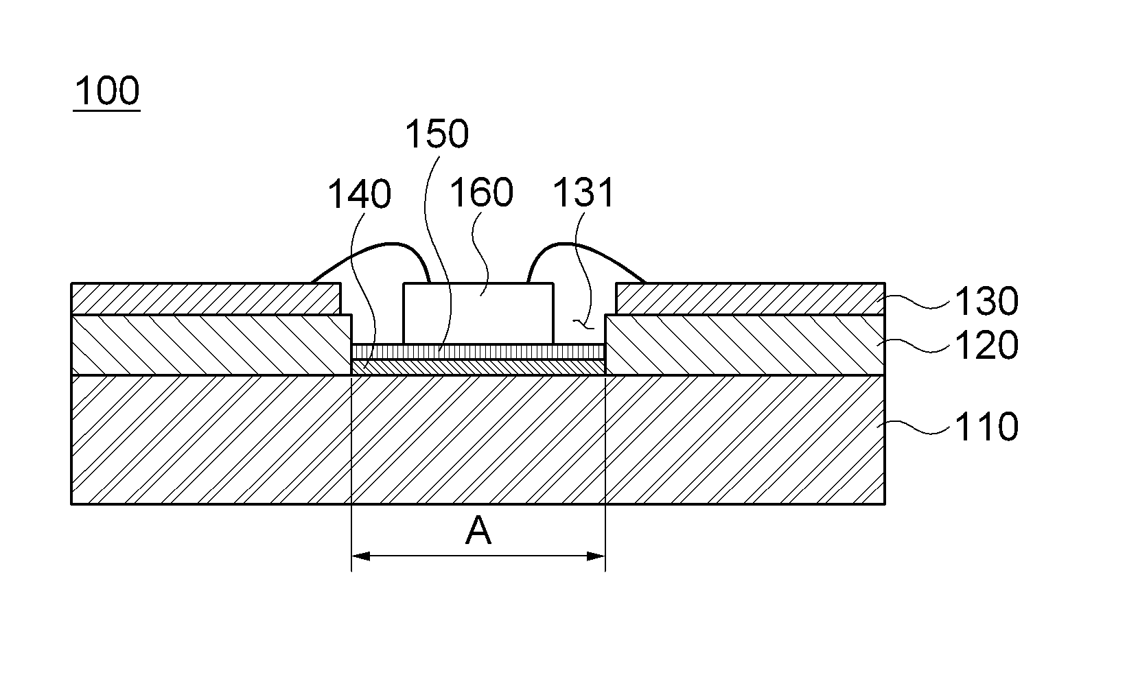
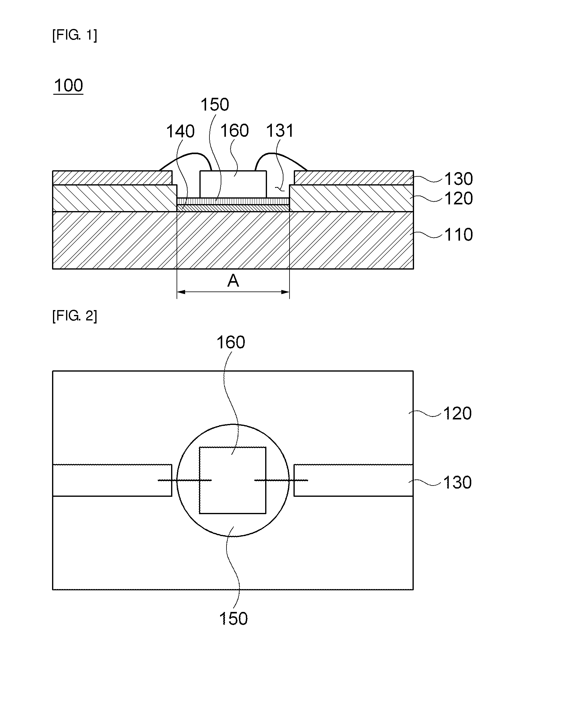
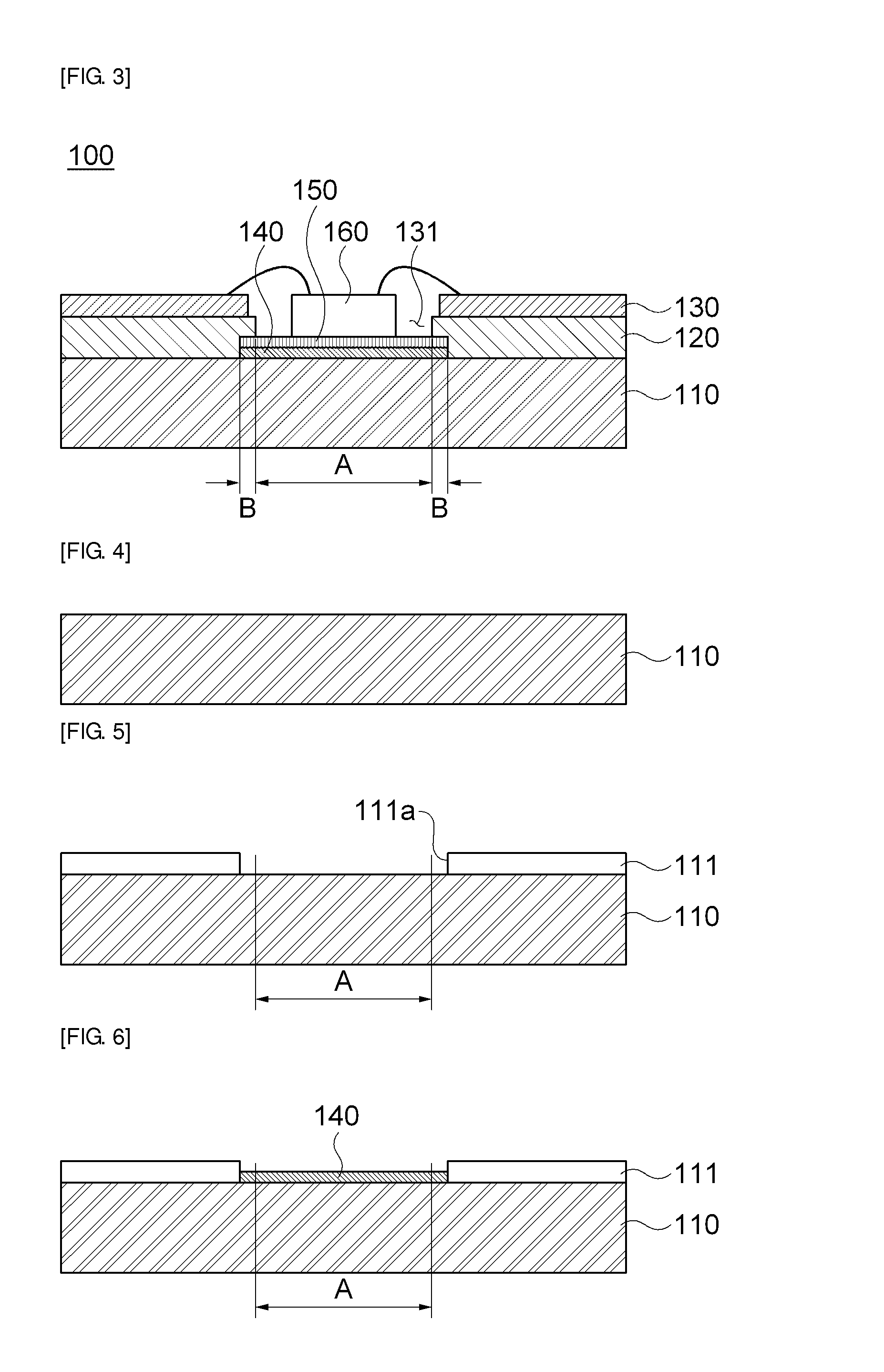
[0042]Embodiments of the present invention for achieving the above objects will be described with reference to the accompanying drawings. In the specification, like reference numerals denote like elements, and duplicate or redundant descriptions will be omitted for conciseness.

[0043]It should be noted that the singular forms ‘a’‘an’ and ‘the’ are intended to include the plural forms as well, unless the context clearly indicates otherwise. It should be understood that the terms ‘comprise’, ‘include’ and ‘have’, when used in this specification, specify the presence of stated features or elements, but do not preclude the presence or addition of one or more other features, elements, or combinations thereof.

[0044]The drawings referred to in the present specification will be described exaggeratedly in a shape, a size, a thickness or the like in order to effectively explain the technical features of the present invention as an example to represent the embodiments of the present in the pres...


PUM

PropertyMeasurementUnit
thicknessaaaaaaaaaa
grain diameteraaaaaaaaaa

Abstract

As a substrate for an LED module and a method for manufacturing the same, they teach a substrate for an LED module and a method for manufacturing the same which including a base substrate, an insulating layer formed on a remaining region except a chip mounting region A in the base substrate, an electrode layer formed on the insulating layer, an oxide layer formed on the chip mounting region A of the base substrate and a high reflection layer formed on a top surface of the oxide layer.

Description

CROSS-REFERENCE TO RELATED APPLICATIONS[0001]This application claims the benefit of Korean Patent Application No. 10-2012-0078806 filed with the Korea Intellectual Property Office on Jul. 19, 2012, the disclosure of which is incorporated herein by reference.BACKGROUND OF THE INVENTION[0002]1. Field of the Invention[0003]The present invention relates to a substrate for a LED module and a method for manufacturing the same; and, more particular, to a substrate for a LED module provided with a high reflection layer and a method for manufacturing the same.[0004]2. Description of the Related Art[0005]In recent, a light emitting diode (hereinafter referred to as LED) has been come into the spotlight as an illumination means or a light emitting means capable of realizing weight lightening, slimness and power saving. The LED device is as a light device to emit lights while applying currents to a pn junction of a semiconductor in a forward and is manufactured by using III-V group semiconducto...

Claims


Application Information

Patent Timeline
Patent Type & Authority Applications(United States)
IPC IPC(8): H05K1/03H05K3/10H05B33/02
CPCH05K1/0306H05B33/02H05K3/108H05K1/0274H01L33/60H05K2201/10106H05K2201/0175H05K2201/2072H05K2201/2054H01L2224/48091H01L2224/45144H01L2924/00014H01L2924/00
Inventor HEO, CHEOL HO
Owner SAMSUNG ELECTRO MECHANICS CO LTD
Learn More