Thin film balun

a thin film balun and transformer technology, applied in the field of balun transformers, can solve the problems of increasing the effective capacitance of the unbalanced circuit side, and achieve the effects of improving the passage characteristics of the thin film balun, excellent passage characteristics, and changing the impedance of the entire circui

Active Publication Date: 2014-01-23
TDK CORPARATION
View PDF6 Cites 1 Cited by
  • Summary
  • Abstract
  • Description
  • Claims
  • Application Information

AI Technical Summary

Benefits of technology

[0010]Though details of a functional mechanism are still unclear, the following assumption can be made. When the part of the line portion constituting the unbalanced circuit serves as the electrode of the capacitor, the capacitor is positioned near the unbalanced circuit. Therefore, not only the capacitance C is introduced directly, but also a capacitance like a stray capacitance is induced with its neighboring line portions, which leads to an increase in effective capacitance on the unbalanced circuit side. Hence, by changing a position or an area of the line portion serving as the electrode of the capacitor, the balance characteristics can be adjusted easily while maintaining desired passage characteristics according to the specifications of the thin film balun. Note, however, that the function is not limited to such.
[0049]According to the fifth aspect of the present invention, the capacitor is introduced between the part of the balanced transmission line and the ground terminal, with it being possible to achieve excellent passage characteristics for the thin film balun which is made smaller and thinner.

Problems solved by technology

Therefore, not only the capacitance C is introduced directly, but also a capacitance like a stray capacitance is induced with its neighboring line portions, which leads to an increase in effective capacitance on the unbalanced circuit side.

Method used


Image

  • Thin film balun
  • Thin film balun
  • Thin film balun

Examples


first embodiment

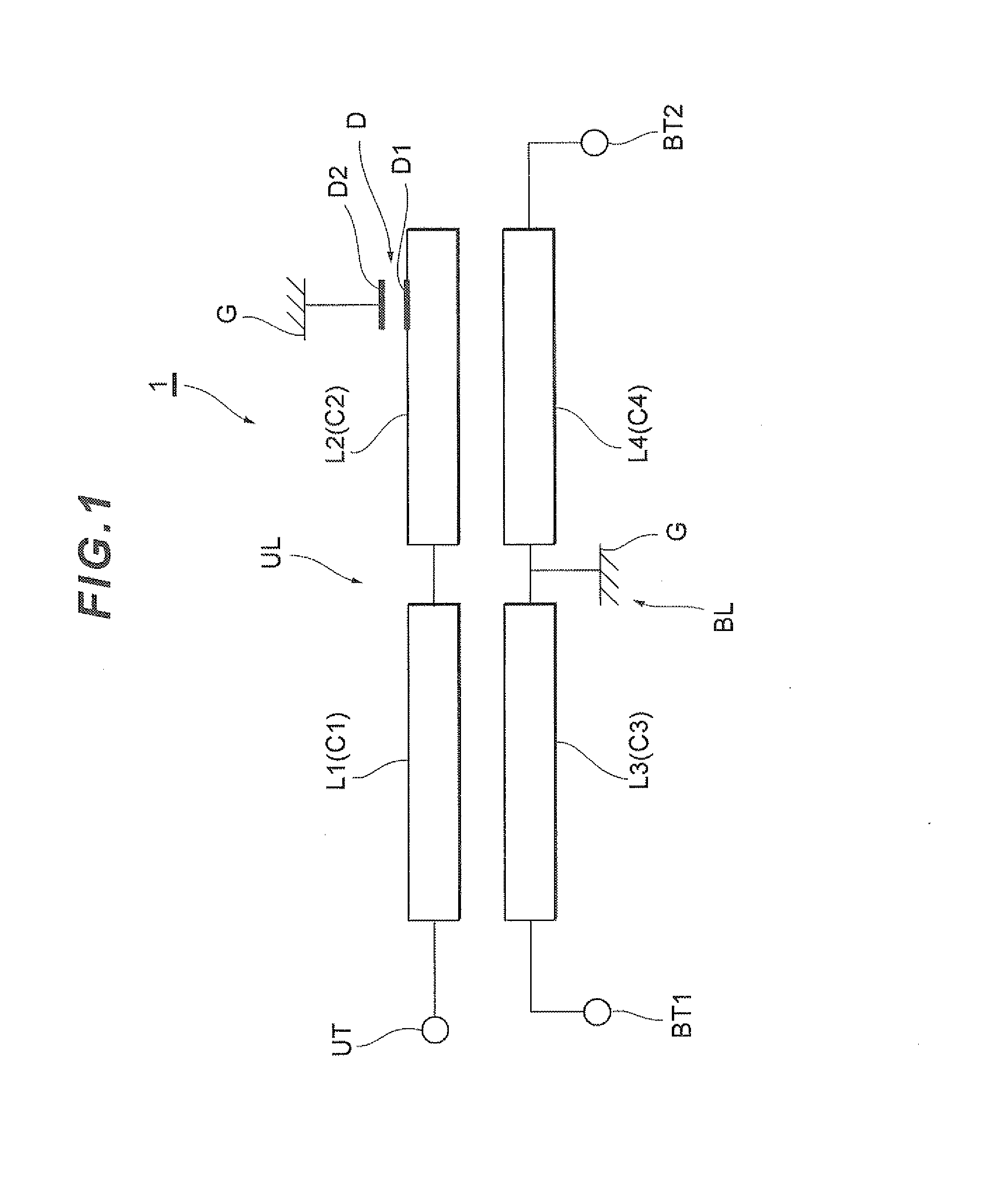
[0164]A thin film balun in a first embodiment corresponding to the first aspect of the present invention is described first. FIG. 1 is an equivalent circuit diagram showing a structure of the thin film balun in the first embodiment of the present invention. A thin film balun 1 includes an unbalanced transmission line (unbalanced circuit) UL in which a line portion L1 (first line portion) and a line portion L2 (second line portion) are connected in series, and a balanced transmission line (balanced circuit) BL in which a line portion L3 (third line portion) and a line portion L4 (fourth line portion) are connected in series. The line portions L1 and L3 form magnetic coupling, and the line portions L2 and L4 form magnetic coupling.

[0165]In the thin film balun 1, an end of the line portion L1 other than an end connected to the line portion L2 is connected to an unbalanced terminal UT, and a part of an end of the line portion L2 other than an end connected to the line portion L1 is conn...

example 2c

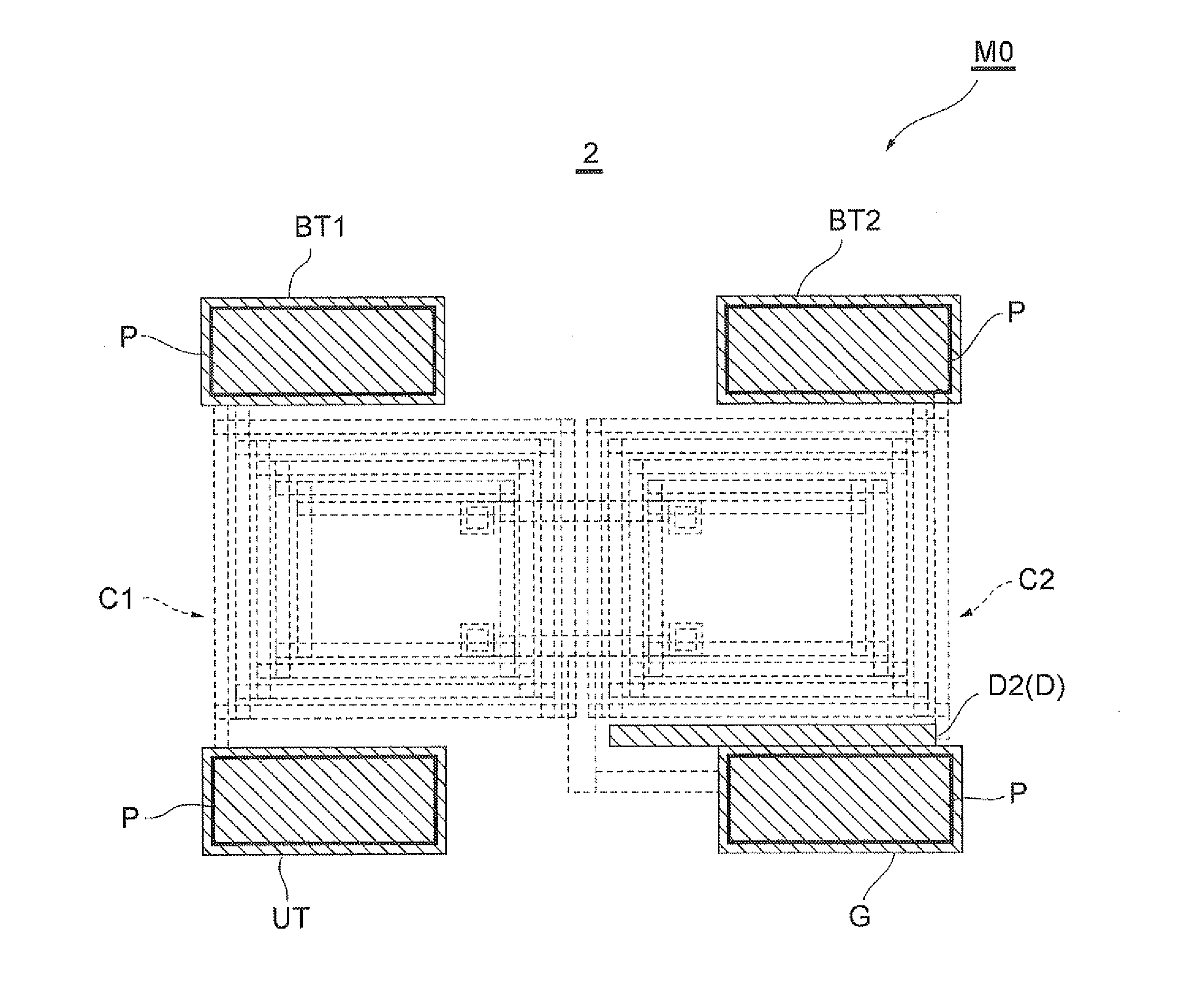
[0189]FIG. 18 is a horizontal sectional view schematically showing the wiring layer M0 of a thin film balun 2C of an example 2C. Structures other than the wiring layer M0 are the same as those in the example 2. In the thin film balun 2C shown in FIG. 18, the electrode D2 of the capacitor D is positioned so as to be parallel to an extending direction of a space between the coil conductor of the first line (the extension 12c) and the coil conductor of the second line from the bottom of the coil portion C2 and face a part of the coil conductors on both sides of the space in plan view.

example 2d

[0190]FIG. 19 is a horizontal sectional view schematically showing the wiring layer M0 of a thin film balun 2D of an example 2D. Structures other than the wiring layer M0 are the same as those in the example 2. In the thin film balun 2D shown in FIG. 19, the electrode D2 of the capacitor D is positioned so as to face a plurality of coil conductors 12 in a lower right region of the coil portion C2. Here, the electrode D2 has the same area as in the examples 2 and 2A to 2C.

[0191](Characteristic Evaluation)

[0192]Passage characteristics (insertion loss) and balance characteristics (phase difference and amplitude difference of balanced signals) of each of the thin film baluns 2 and 2A to 2D of the examples described above were measured by simulation. Evaluation target frequencies (resonant frequencies fr) of a transmission signal were set at 2400 MHz to 2500 MHz. FIG. 20 is a diagram showing passage characteristic evaluation results, FIG. 21 is a diagram showing phase difference evaluati...


PUM


Abstract

A thin film balun that can be made smaller and thinner while maintaining required balun characteristics is provided. A thin film balun 1 includes: an unbalanced transmission line UL including a first coil portion C1 and a second coil portion C2; a balanced transmission line BL including a third coil portion C3 and a fourth coil portion C4 that are positioned facing and magnetically coupled to the first coil portion C1 and the second coil portion C2 respectively; an unbalanced terminal UT connected to the first coil portion C1; a ground terminal G connected to the second coil portion C2 via a C component D; and an electrode D2 connected to the ground terminal G and facing a part of the second coil portion C2. The C component D is formed by the electrode D2 and the part D1 of the second coil portion C2.

Description

CROSS REFERENCE TO RELATED APPLICATION[0001]This application is a divisional application of U.S. application Ser. No. 12 / 823,450, filed Jun. 25, 2010 and claims the benefit of Japanese Application Nos. 2009-156239 filed on Jun. 30, 2009, No. 2009-157726 filed on Jul. 2, 2009, No. 2009-156241 filed on Jun. 30, 2009, No. 2009-192593 filed on Aug. 21, 2009 and No. 2009-192594 filed on Aug. 21, 2009, which are incorporated herein by reference.BACKGROUND OF THE INVENTION[0002]1. Field of the Invention[0003]The present invention relates to a balun (balun transformer) that performs conversion between unbalanced and balanced signals, and in particular relates to a thin film balun that is formed by a thin film process advantageous for smaller and thinner models.[0004]2. Description of the Related Art[0005]A wireless communication device includes various high frequency elements such as an antenna, a filter, an RF switch, a power amplifier, an RF-IC, and a balun. Of these elements, a resonant ...

Claims


Application Information

Patent Timeline
Patent Type & Authority Applications(United States)
IPC IPC(8): H01P5/10
CPCH01P5/10H03H7/422H03H2001/0078
Inventor ENDO, MAKOTO
Owner TDK CORPARATION
Why Eureka
Try Eureka