Quantum dot array capacitor and preparation method thereof

A technology of capacitors and quantum dots, applied in capacitors, electric solid devices, circuits, etc., can solve the problem of small capacitance density of capacitors

Active Publication Date: 2020-10-30
SIEN QINGDAO INTEGRATED CIRCUITS CO LTD
View PDF5 Cites 0 Cited by
  • Summary
  • Abstract
  • Description
  • Claims
  • Application Information

AI Technical Summary

Problems solved by technology

[0005] In view of this, an embodiment of the present invention provides a quantum dot array capacit...

Method used


Image

  • Quantum dot array capacitor and preparation method thereof
  • Quantum dot array capacitor and preparation method thereof
  • Quantum dot array capacitor and preparation method thereof

Examples


Embodiment Construction

[0070] In order to make the purpose, technical solutions and advantages of the embodiments of the present invention clearer, the technical solutions in the embodiments of the present invention will be clearly and completely described below in conjunction with the drawings in the embodiments of the present invention. Obviously, the described embodiments It is a part of embodiments of the present invention, but not all embodiments. Based on the embodiments of the present invention, all other embodiments obtained by those skilled in the art without creative efforts fall within the protection scope of the present invention.

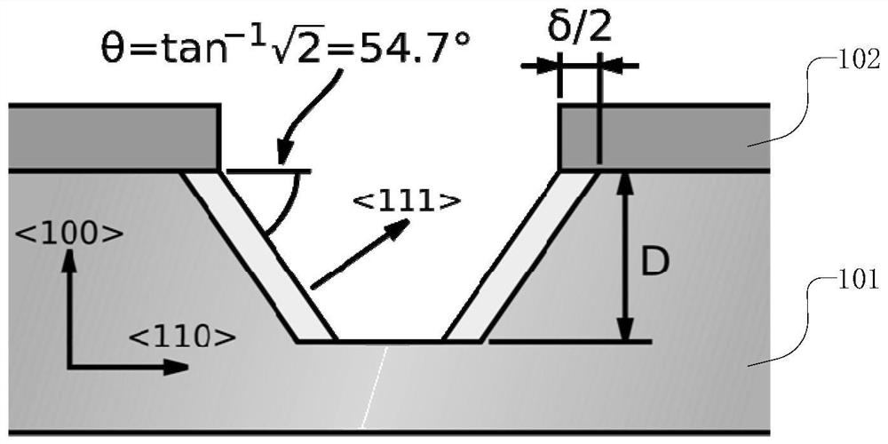
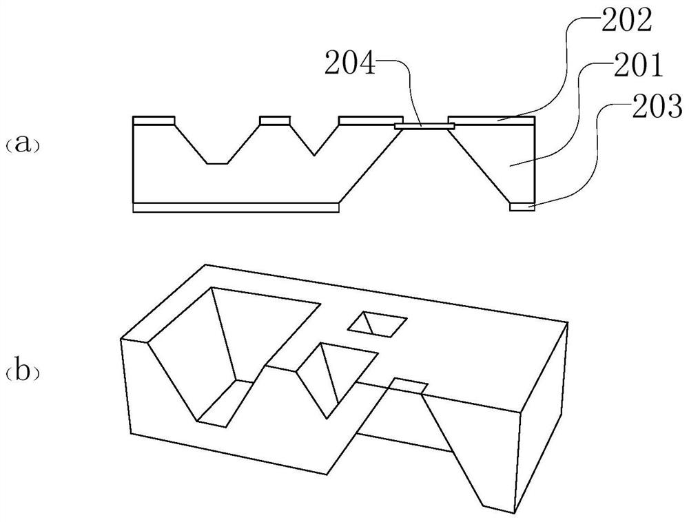
[0071] The invention provides a quantum dot array capacitor, the capacitor includes a multilayer pyramid array, and the capacitor includes a semiconductor substrate. In semiconductor manufacturing technology, commonly used semiconductor substrates include silicon wafers. The crystal of silicon has a diamond-like structure, and the silicon atoms inside the cr...


PUM


Abstract

The invention provides a quantum dot array capacitor and a preparation method thereof. The capacitor comprises a semiconductor substrate, a first conductive layer located on the semiconductor substrate, a first dielectric layer located on the first conductive layer, a second conductive layer located on the first dielectric layer and a second dielectric layer located on the second conductive layer.Conductive layers and dielectric layers are and alternately formed to obtain a multi-layer capacitor structure. The capacitor is formed into a multi-layer pyramid-shaped array. Due to the fact that the pyramid array structure is adopted in the array capacitor, larger capacitance is generated on the same wafer area; and the conductive layers and the dielectric layers can be repeatedly formed, so that the capacitance density per unit area can be further improved.

Description

technical field [0001] The invention relates to the technical field of semiconductors, in particular to a quantum dot array capacitor and a preparation method thereof. Background technique [0002] In the field of semiconductor technology, capacitors are widely used as basic components for filtering, decoupling, bypassing and other uses. [0003] In the existing capacitor manufacturing process, an insulating layer, a bottom electrode layer, a dielectric layer, and a top electrode layer are usually sequentially formed on a semiconductor substrate, and a barrier layer, a passivation layer, etc. can be formed on the top electrode layer. electrical connections between the bottom electrode layers. The capacitors prepared by the above method occupy a considerable part of the space on the wafer. In addition, a wiring structure for connecting the capacitor to an external circuit needs to be provided, which further increases the space occupied by the capacitor on the surface of the...

Claims


Application Information

Patent Timeline
IPC IPC(8): H01L23/64
CPCH01L28/40
Inventor 王津洲张汝京
Owner SIEN QINGDAO INTEGRATED CIRCUITS CO LTD
Why Eureka
Try Eureka