Integrated Power Passives

a technology of integrated devices and power passives, which is applied in the manufacture of capacitors, semiconductor/solid-state devices, printed circuit non-printed electric components, etc., can solve the problems of mechanical robustness, limit the achievable, and no known practical fabrication techniques for fabricating power passives with high energy density. achieve the effect of high capacitance and aid in heat dissipation

Inactive Publication Date: 2010-01-28
UNIV OF FLORIDA RES FOUNDATION INC
View PDF12 Cites 18 Cited by
  • Summary
  • Abstract
  • Description
  • Claims
  • Application Information

AI Technical Summary

Benefits of technology

[0008]A multilayer film-stack, includes a substrate; a series of alternating dielectric and electrically conducting layers disposed on the substrate, wherein the area of the layers monotonically decreases as a distance from the substrate increases; and electrical connections coupled to two or more of the conducting layers. The individual conducting layers can be two or more different conducting materials. The multilayer film-stack can be a programmable capacitor. The programmable capacitor can further include an electrical circuit disposed on the substrate having an output coupled to the capacitor. The electrical circuit coupled to the capacitor can be a voltage regulator. The voltage regulator can be a dc-dc voltage regulator. The device can also include an inductor formed on the substrate with the inductor coupled to the capacitor.
[0009]A method for forming a multilayer film-stack including the steps of: providing a substrate; forming at least one plateau region on the substrate; depositing a series of alternating dielectric layers and conducting material layer on the substrate including over the plateau regions where the first and last layers can be selected to be either a dielectric layer or a conducting material layer, and the dielectric layers can be the same or different materials and the conducting material layers can be the same or different materials; removing the top surface to expose at least one of the plateaus and two or more edges of the conducting material layers; addressing two or more of the edges selectively in the vicinity of at least one of the plateaus; and depositing selectively at least one connecting conductive layer contacting some or all of the selected edges such that electrical connectivity can be made in and out of the multilayer film-stack. The step of removing can involve removal processes including mechanical polishing, chemical mechanical planarization, electric discharge machining or ion milling. Particularly for thin layers of about 50 nm or less, the step of addressing can include the steps of: etching a portion of the edges of a selected conducting material when two or more conducting materials are deposited; depositing a dielectric layer wherein the voids resulting from etching are filled; and removing the dielectric to expose the edges of the conductive material that was not etched. Alternately for thicker layers of about 100 nm or more, the step of addressing can be a photolithographic process. The connecting conductive layer can be selectively deposited by sputtering a conducting material using a shallow mask on the area above selected plateaus.
[0010]The method of forming a multilayer film-stack can be used to form high capacitance density capacitors when the step of depositing a series of the dielectric layers and the conducting material layers are repeated wherein the dielectric layer, a first conducting material, the dielectric layer, and a second conducting material are successively deposited until a predetermined number of dielectric layers and conducting material layers have been deposited. The first and second conducting materials can be chosen to have different properties such as etching rates and can be, for example, aluminum and titanium, respectively. Furthermore, a feature that is an electrically conductive material can be selectively deposited on the area and around at least one of the plateaus by sputtering using a shadow mask.
[0011]The formation of the capacitor by the method of forming a multilayer film-stack can be included in the formation of a power system-on-a-chip (SoC) that including at least one transistor, at least one conductor, at least one inductor and at least one capacitor, where the substrate and the one or more plateaus are features of an inductor formed by the steps of: providing a complementary metal oxide semiconductor (CMOS) circuit having a frontside oxide layer having at least one metal layer disposed therein and having a backside silicon layer; forming at least one trench originating from the backside of the substrate through the substrate to the frontside oxide layer; depositing a dielectric coating on the walls of the trench; etching anisotropically the dielectric coating and oxide layer at the base of the trenches to expose at least one of the disposed metals in the frontside oxide layer; depositing a magnetic core material in the trenches, wherein the dielectric coating surrounds the core material. The method also includes a dielectric layer on the backside surface including the exposed core material; etching from the backside at least one portion of dielectric layer, the silicon layer and anisotropically etching the adjacent frontside oxide layer to expose at least one metal layer deposited on the frontside oxide layer to form open channels surrounding the core material; and depositing a metal in the open channels surrounding the core material, wherein an inductor is formed with the metal extending to the metal disposed in the frontside oxide layer and where the backside ends of the metal are the plateaus. Steps can be included to pre-treating any of the exposed metals prior to the deposition of the metal where pre-treatment is the formation of an adhesion layer over the exposed portion of the metal. Steps to frontside etch the oxide to reveal exposed metal; and deposit a metal onto the exposed metal can be included. Steps to form at least one deep trench originating from the backside of the substrate into or through the substrate and optionally through the oxide to metal disposed in the oxide layer; and to deposit a metal in the trench can be included to form a thermal plug to aid in heat dissipation from the SoC. A step to planarize the backside surface after depositing the magnetic core material can be included. The magnetic core material can be permalloy.

Problems solved by technology

There are presently no known practical fabrication techniques for fabricating power passives with high energy density.
There are many issues to be solved with MEMS inductors.
Silicon-based micro-inductors offer the advantage of integratability with active electronics, but substrate loss and parasitic capacitances limit the achievable Q. Mechanical robustness is a concern if the substrate is removed or the microstructure is hung above or out of the substrate, where packaging difficulties must be addressed.
Fabrication using microwave plasma ashing to remove thick polymer (>150 μm) such as SU-8 is time-consuming and can have undesired side effects especially on CMOS substrates.
Because of the skin effect, increasing the copper line width may not yield low ac resistance at high frequency.
This approach to is very complicated and very expensive.
Hence, the goal of an integrated dc-dc converter with improved power density remains unfulfilled.

Method used


Image

  • Integrated Power Passives
  • Integrated Power Passives
  • Integrated Power Passives

Examples


Embodiment Construction

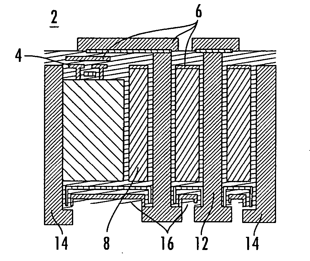
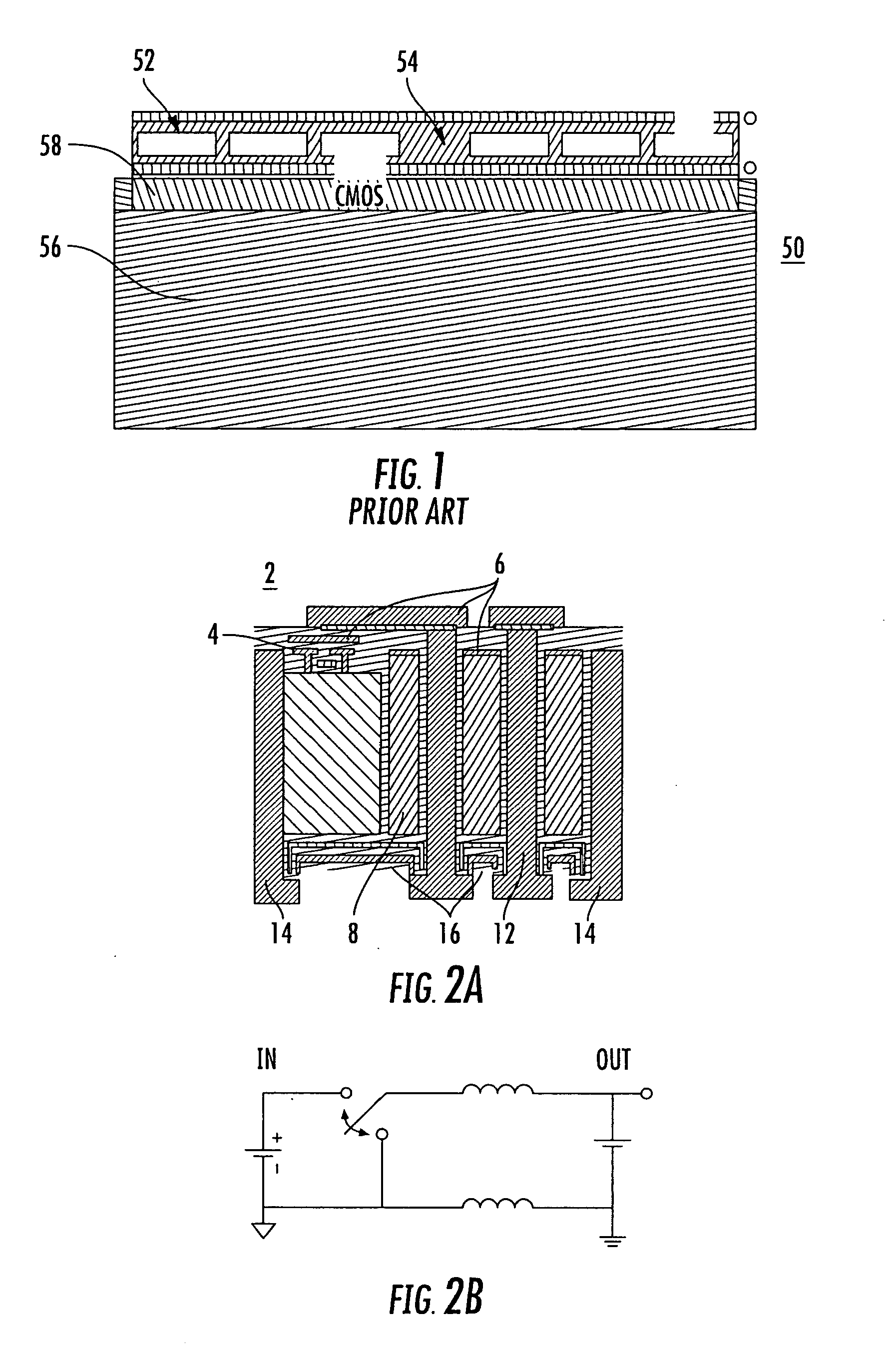
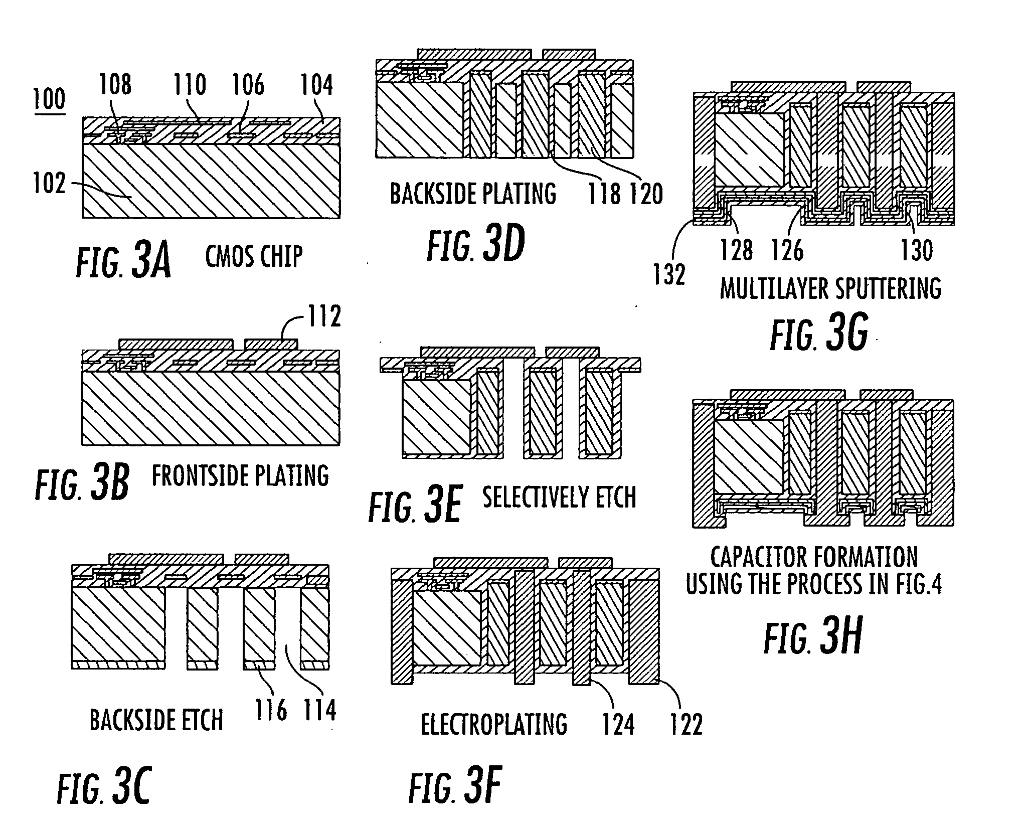
[0018]The invention involves a new fabrication process and associated devices that are CMOS-compatible and enable monolithic integration of high-Q, high-inductance, high-current-handling inductors and high-density capacitance capacitors, such as for power electronic circuits. The invention is enabled by a novel process to prepare a multilayer film-stack such that a stack of conducting layers separated by dielectric layers are formed over a substrate having one or more elevated plateaus above a surface of the substrate and upon removing a portion of the layers generally to about the surface of at least one of the plateaus, which permits the selective addressing of conducting layers. Selective addressing as used herein is the connection of some but not all of the conductive layers. For very thin layers, selective addressing can be carried out by using two or more different conducting layers and selectively etching one or more of the conducting layers and effectively filling the volume...


PUM


Abstract

A multi-layer film-stack and method for forming the multilayer film-stack is given where a series of alternating layers of conducting and dielectric materials are deposited such that the conducting layers can be selectively addressed. The use of the method to form integratable high capacitance density capacitors and complete the formation of an integrated power system-on-a-chip device including transistors, conductors, inductors, and capacitors is also given.

Description

CROSS-REFERENCE TO RELATED APPLICATIONS[0001]This application is the U.S. national stage application of International Patent Application No. PCT / US2007 / 065773, filed Apr. 2, 2007, which claims the benefit of U.S. Provisional Patent Application Ser. No. 60 / 788,034, filed Mar. 31, 2006, the disclosures of which are incorporated by reference herein in their entirety, including any figures, tables, or drawings.FIELD OF THE INVENTION[0002]The invention relates to the fabrication of multilayer film-stack, high energy density capacitors, and integrated devices therefrom.BACKGROUND[0003]Monolithic integration has emerged to reduce cost and to improve transient performance of power converters including dc-dc converters. There have been feasibility studies, and calculations suggested that power density exceeding 1000 W / cm2 is feasible at efficiency above 80%. State-of-the-art power density, however, currently has not exceeded 20 W / cm2 at output power above 10 W. To increase the power density ...

Claims


Application Information

Patent Timeline
Patent Type & Authority Applications(United States)
IPC IPC(8): H01G4/30B44C1/22H05K1/00
CPCH01G4/33H01L23/3677H01L28/40H01L2924/0002H01L2924/00
Inventor XIE, HUIKAINGO, KHAI
Owner UNIV OF FLORIDA RES FOUNDATION INC
Why Eureka
Try Eureka